Dual pinned diode pixel with shutter

a diode pixel and shutter technology, applied in the field of semiconductor imagers, can solve the problems of difficult control, capacitor use, and inability to accurately control the operation of the rolling shutter,

Active Publication Date: 2011-12-06
MICRON TECH INC
View PDF19 Cites 16 Cited by
  • Summary
  • Abstract
  • Description
  • Claims
  • Application Information

AI Technical Summary

Problems solved by technology

The above described rolling shutter operation is not suitable for imaging scenes with objects having significant motion because each row is effectively imaged at a different time.
Some imagers utilize mechanical shutters, which may be difficult to control precisely.
Although electronic shutters can be more easily controlled, the use of capacitors has some disadvantages including, for example, a decreased pixel fill factor, decreased efficiency in pixel charge transfer, and increased susceptibility to noise.

Method used


Image

  • Dual pinned diode pixel with shutter
  • Dual pinned diode pixel with shutter
  • Dual pinned diode pixel with shutter

Examples


Embodiment Construction

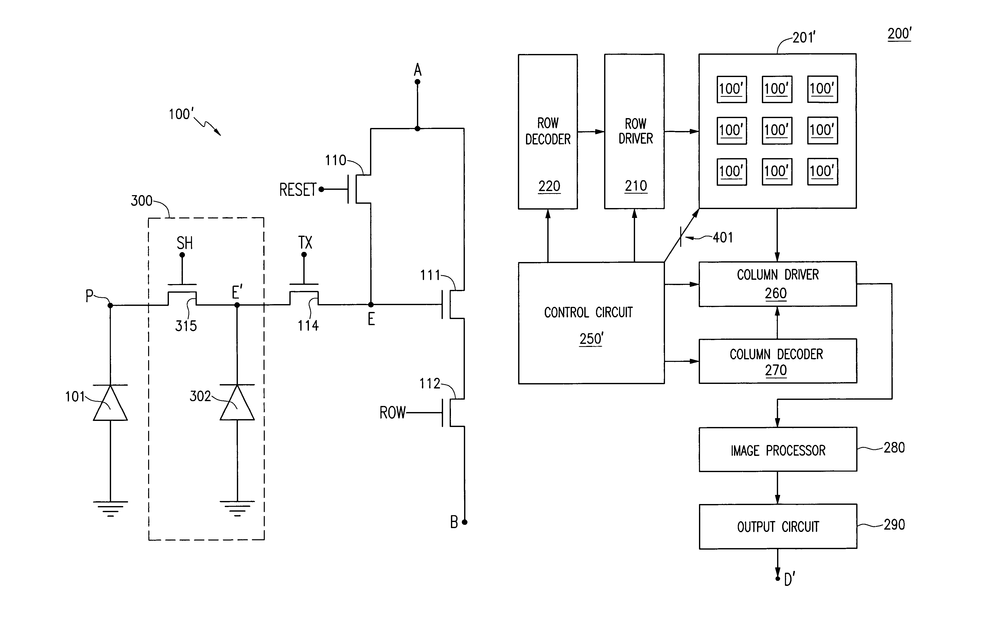
[0017]Now referring to the drawings, where like reference numerals designate like elements, there is shown in FIG. 3, a pixel 100′ having an architecture in accordance with one embodiment of the invention. The pixel 100′ includes several components found in pixel 100 (FIG. 1), but the illustrated pixel 100′ includes additional circuitry in the form of an electronic shutter 300.

[0018]Node A of the pixel 100′ is coupled to a voltage source, which is typically a pixel array supply voltage VAAPIX. Node B is an output node. The pixel 100′ outputs its reset signal Vrst and the photo signal Vsig, at different times through node B.

[0019]The photodiode 101 is typically a pinned photodiode, and produces photo generated charges, the number of which varies in accordance with incident light. The photo generated charges accumulate at node P. Typically, the incident light arrives from a subject after being focused by a lens assembly (not illustrated).

[0020]The electronic shutter 300 includes a pin...


PUM


Abstract

A pixel having an electronic shutter suitable for use in a pixel array of an imaging device includes a pinned diode and a shutter transistor. The pinned diode is utilized as a storage device while the shutter transistor controls charge transfer from the electronic shutter. The use of a pinned diode as a charge storage device for the electronic shutter permits greater charge transfer efficiency, has lower leakage (or “dark” current), and permits the resulting pixel to have a greater fill factor than pixels utilizing conventional electronic shutter circuits.

Description

FIELD OF INVENTION[0001]The present invention relates generally to semiconductor imagers. More specifically, the present invention relates to a pixel architecture supporting an electronic shutter.BACKGROUND OF THE INVENTION[0002]FIG. 1 illustrates a conventional four transistor (4T) imager pixel 100 coupled via interconnect 125 to a conventional pixel reading circuit 150. The pixel 100 includes a photodiode 101, reset, source follower, row select, and transfer transistors 110-114, and nodes A, B, E, and P. Control signals RESET, TX, and ROW are respectively applied to the gates of the reset transistor 110, the transfer transistor 114, and the row select transistor 112. Node A is connected to a supply voltage source (VAAPIX) for the pixel 100. Node E is a charge storage node. Node P is a charge accumulation node of the photodiode 101. The outputs produced by the pixel 100 are made available at node B. These outputs include a reset output voltage Vrst and a pixel image signal output v...

Claims


Application Information

Patent Timeline
Patent Type & Authority Patents(United States)
IPC IPC(8): H04N3/14H01L27/00H04N5/335
CPCH04N5/353H04N5/37452H04N25/53H04N25/771
Inventor RYSINSKI, JEFFREY
Owner MICRON TECH INC
Why Eureka
Try Eureka