Eureka AIR delivers breakthrough ideas for toughest innovation challenges, trusted by R&D personnel around the world.

Substrate processing apparatus and method of manufacturing semiconductor device

a processing apparatus and semiconductor technology, applied in the field of substrate processing apparatus and a manufacturing method of semiconductor devices, can solve the problems of metal contamination in the metal manifold, metal emission from the metallic manifold used in the cvd apparatus becomes an issue, and the bolt or the manifold made of the non-metal component breaks, so as to suppress the collapse of the inner tube, suppress the adhesion of reaction products, and suppress metal contamination in the substrate

Active Publication Date: 2011-12-13
KOKUSA ELECTRIC CO LTD
View PDF5 Cites 13 Cited by
  • Summary
  • Abstract
  • Description
  • Claims
  • Application Information

AI Technical Summary

Benefits of technology

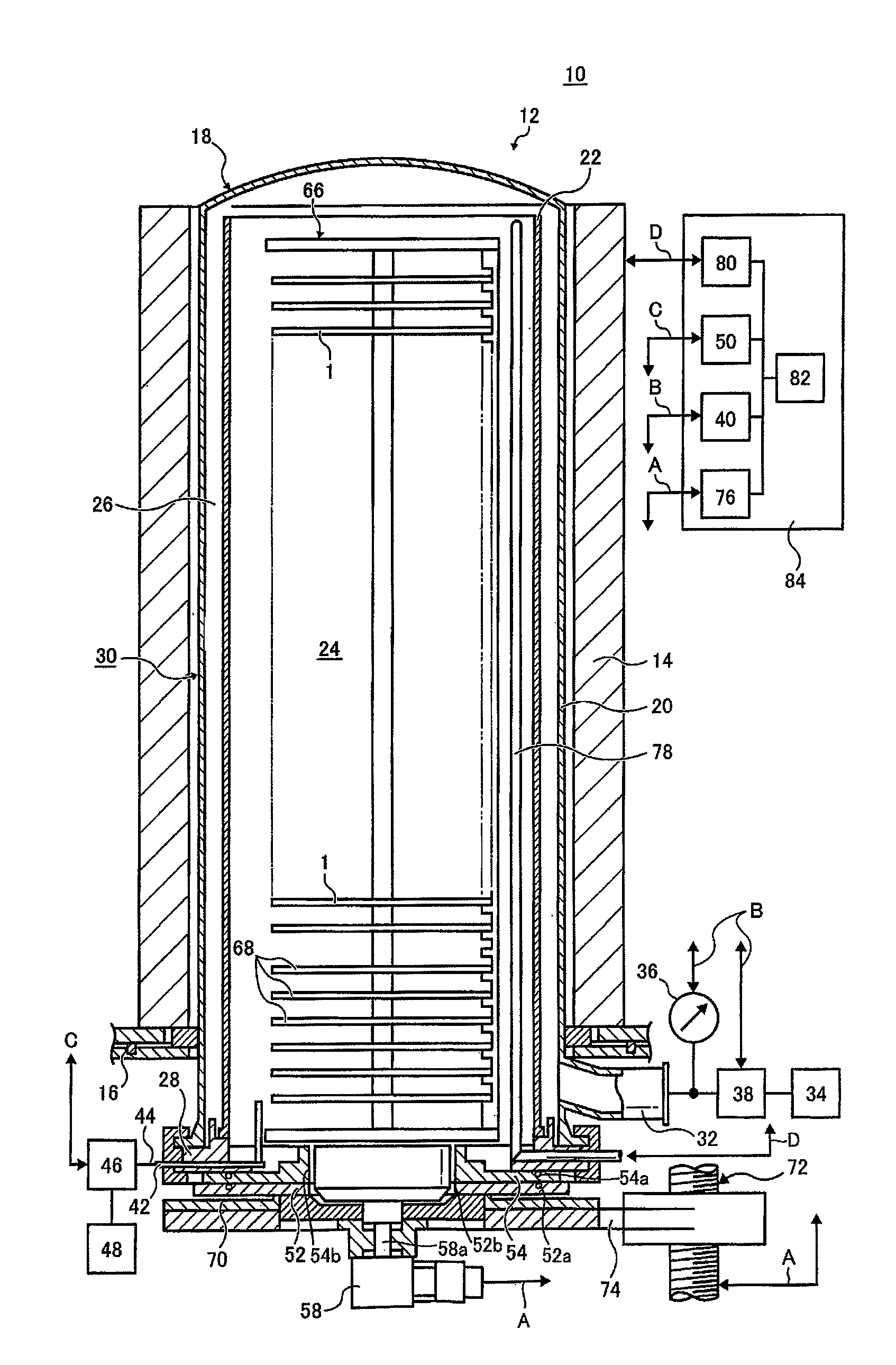
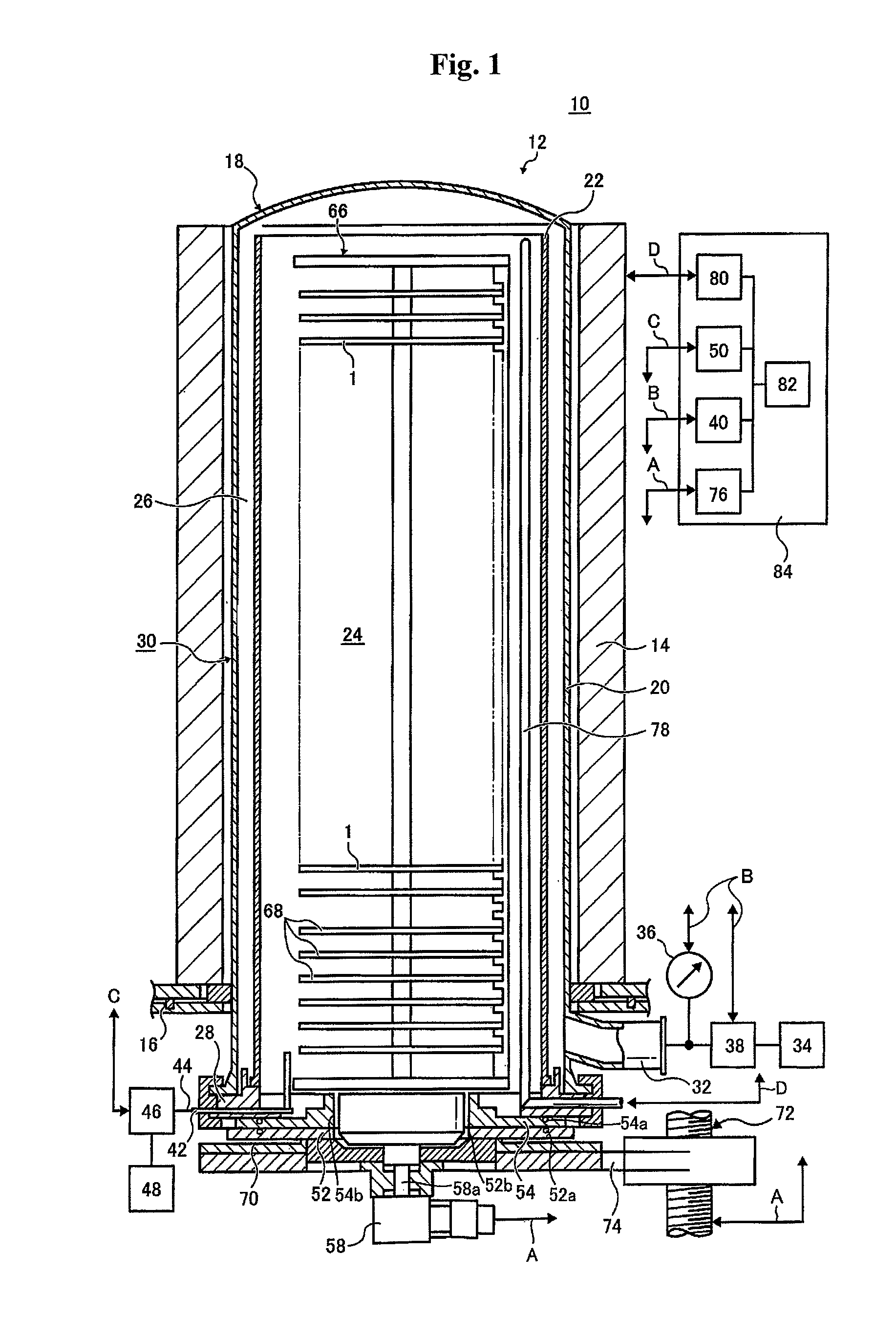
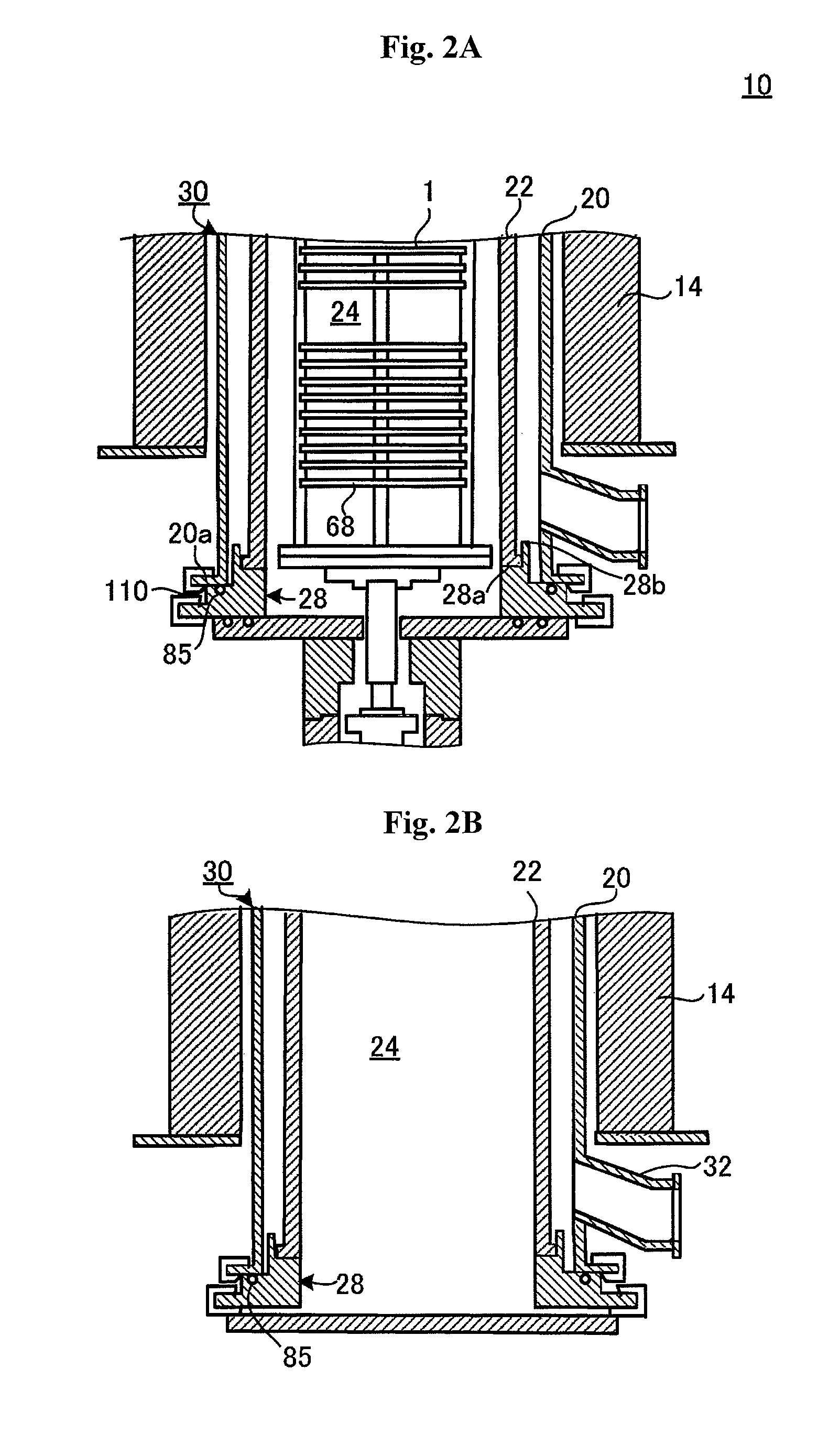
[0014]An object of the present invention is to provide a substrate processing apparatus, which is capable of suppressing metal contamination in a substrate, suppressing collapse of an inner tube, and also suppressing adhesion of reaction products, and to provide a method of manufacturing a semiconductor device.

Problems solved by technology

However, the CVD apparatus using the metallic manifold has a problem in that the metallic manifold is corroded by attachment of reaction products that are generated by a reaction gas and a cleaning gas.
Moreover, as ICs are miniaturized, metal emission from the metallic manifold used in the CVD apparatus becomes an issue.
If the inner tube collapse suppression member is forcibly detached in such a state that the reaction product is adhered thereto, a new problem arises which breaks the bolt or the manifold made of the non-metal component such as quartz.
If the bolt is broken and thus could not be taken away from the manifold, or the manifold is broken, the expensive manifold must be replaced or remanufactured.

Method used


Image

  • Substrate processing apparatus and method of manufacturing semiconductor device
  • Substrate processing apparatus and method of manufacturing semiconductor device
  • Substrate processing apparatus and method of manufacturing semiconductor device

Examples


second embodiment

[0093]FIG. 7A and FIG. 7B illustrate an installation example of the heat insulation cylinder 90 in the present invention.

[0094]In the second embodiment, a lower cylinder part 90c is provided as a movement restriction member protruding downward from the outer periphery of the bottom surface 90a of the heat insulation cylinder 90 in a vertical direction. The lower cylinder part 90c of the heat insulation cylinder 90 is inserted into a groove 28d formed in the second placement part 28b of the manifold 28. Therefore, the horizontal movement and the oblique upward movement of the heat insulation cylinder 90 are suppressed. At the same time, since the horizontal movement of the inner tube 22 is suppressed by the lower cylinder part 90c of the heat insulation cylinder 90 and the groove 28d formed in the second placement part 28b, the oblique upward movement of the heat insulation cylinder 90 is also suppressed. Preferably, the relationship between the thickness A of the cylinder part 90c a...

third embodiment

[0096]In the present invention, as illustrated in FIG. 8, the height of the heat insulation cylinder 90 is set, from the top end to the bottom end of the heater 40, to be higher than the height of shielding the heating wire of the heating element, so that the heating wire of each heater 14, that is, the heating element, does not directly reach the third seal member 85. That is, the heat insulation cylinder 90 is set to be higher than the wire (heating wire) connecting the top end 14a of the heater 14 and the third seal member 85. In this manner, the temperature rise of the third seal member 85 is suppressed.

fourth embodiment

[0097]Herein, when the heat insulation cylinder 90 is provided, the temperature of the exhaust pipe 32 located at a position far from the center of the furnace becomes low and thus by-product may be adhered thereto. In the present invention, as illustrated in FIG. 9, a region facing the exhaust pipe 32 of the heat insulation cylinder 90 is notched upward to form a notch part 90d. Therefore, the heating wire of the heater 14 is partially received in the exhaust pipe 32, and the temperature of the exhaust pipe 32 partially rises. Hence, adhesion of by-product to the exhaust pipe 32 is prevented. Particularly, since the exhaust passage is curved at the lower part around an exhaust port inside the exhaust pipe 32, by-product is easily adhered. However, if the height of the bottom surface of the notch of the notch part 90d is set at the lower part around the exhaust port of the exhaust pipe 32 so high that the heating wire of the heater 14 directly arrives, adhesion of by-product is furt...


PUM

PropertyMeasurementUnit
temperaturesaaaaaaaaaa
temperatureaaaaaaaaaa

Abstract

A substrate processing apparatus comprises: an outer tube; a manifold connected to the outer tube and made of a non-metal material; an inner tube disposed in the manifold at a more inner side than the outer tube and configured to process a substrate therein; a heating device installed at a more outer side than the outer tube and configured to heat the inside of the outer tube; a lid configured to open and close an opening of the manifold, with a seal member intervened therebetween; and a heat absorption member installed in the manifold, with a bottom end of the inner tube intervened therebetween, and configured to absorb heat from the heating device, the heat absorption member being made of a non-metal material.

Description

CROSS-REFERENCE TO RELATED PATENT APPLICATION[0001]This U.S. non-provisional patent application claims priority under 35 U.S.C. §119 of Japanese Patent Application Nos. 2008-218003, filed on Aug. 27, 2008, and 2009-165679, filed Jul. 14, 2009, in the Japanese Patent Office, the entire contents of which are hereby incorporated by reference.BACKGROUND OF THE INVENTION[0002]1. Field of the Invention[0003]The present invention relates to a substrate processing apparatus and a method of manufacturing a semiconductor device.[0004]2. Description of the Prior Art[0005]As one example of a substrate processing apparatus, a semiconductor manufacturing apparatus is known. In particular, as one example of the semiconductor manufacturing apparatus, a vertical diffusion and Chemical Vapor Deposition (CVD) apparatus is known.[0006]The vertical diffusion and CVD apparatus includes: an outer tube; an inner tube installed inside the outer tube to form a process chamber; a heating device (heater) confi...

Claims


Application Information

Patent Timeline
Patent Type & Authority Patents(United States)
IPC IPC(8): F27B5/14C23C16/00
CPCH01L21/67109C23C16/4401
Inventor MORITA, SHINYASADA, KOICHINAKADA, TAKAYUKIMATSUDA, TOMOYUKI
Owner KOKUSA ELECTRIC CO LTD
Why Eureka
Eureka Blog
Learn More