

Substrate processing apparatus and method of manufacturing semiconductor device
- Summary
- Abstract
- Description
- Claims
- Application Information
AI Technical Summary
Benefits of technology
Problems solved by technology
Method used
Image

Examples
second embodiment
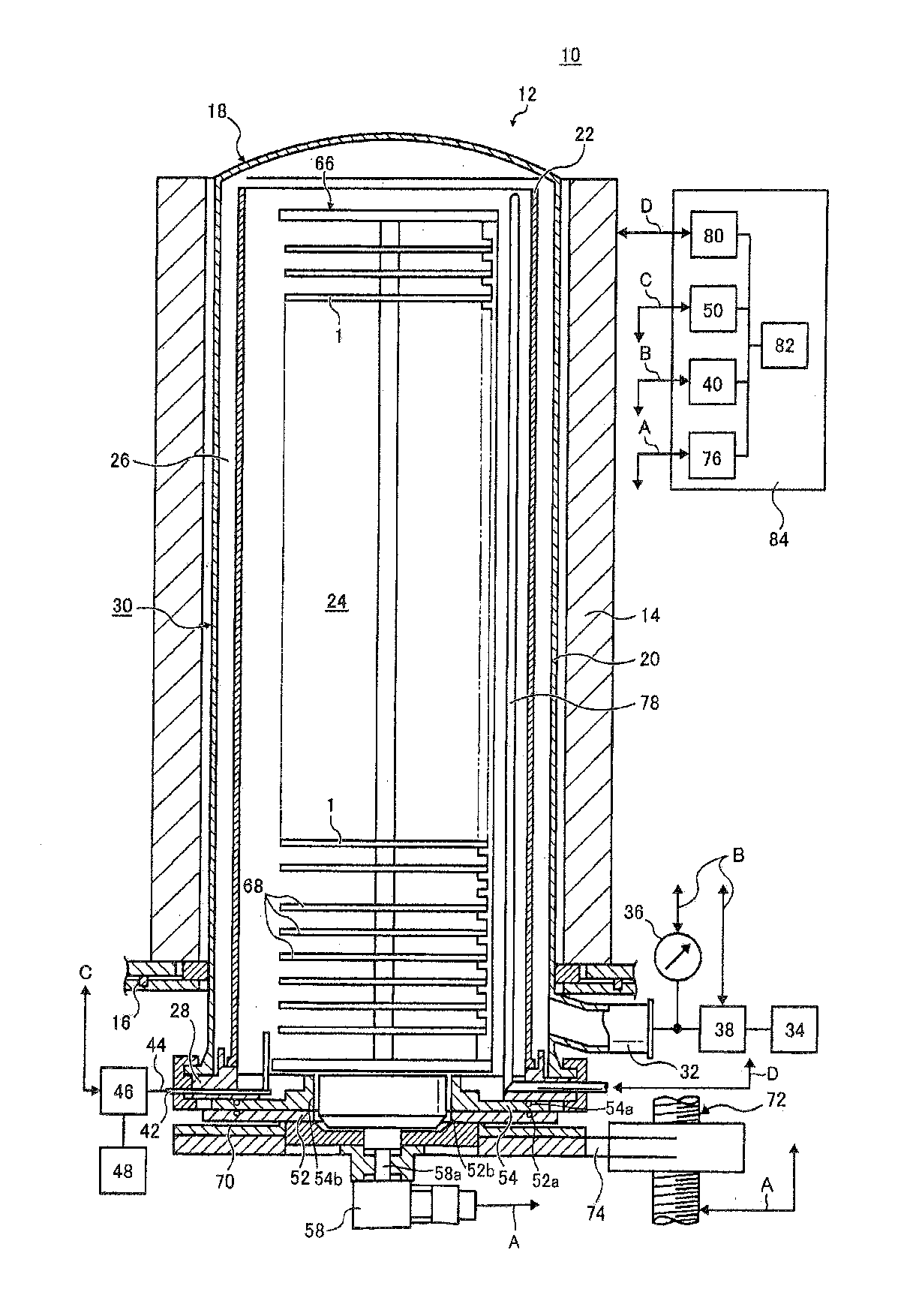
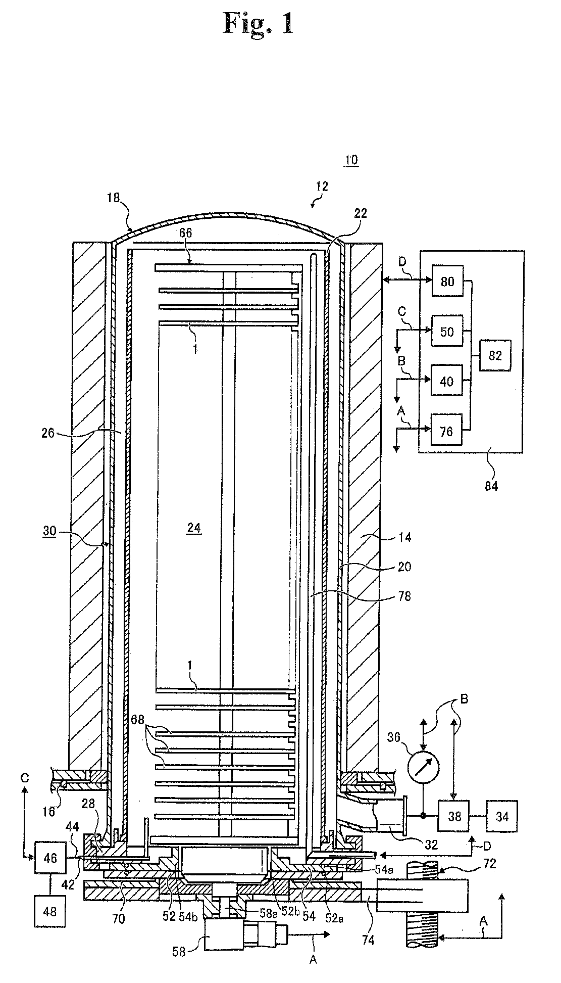
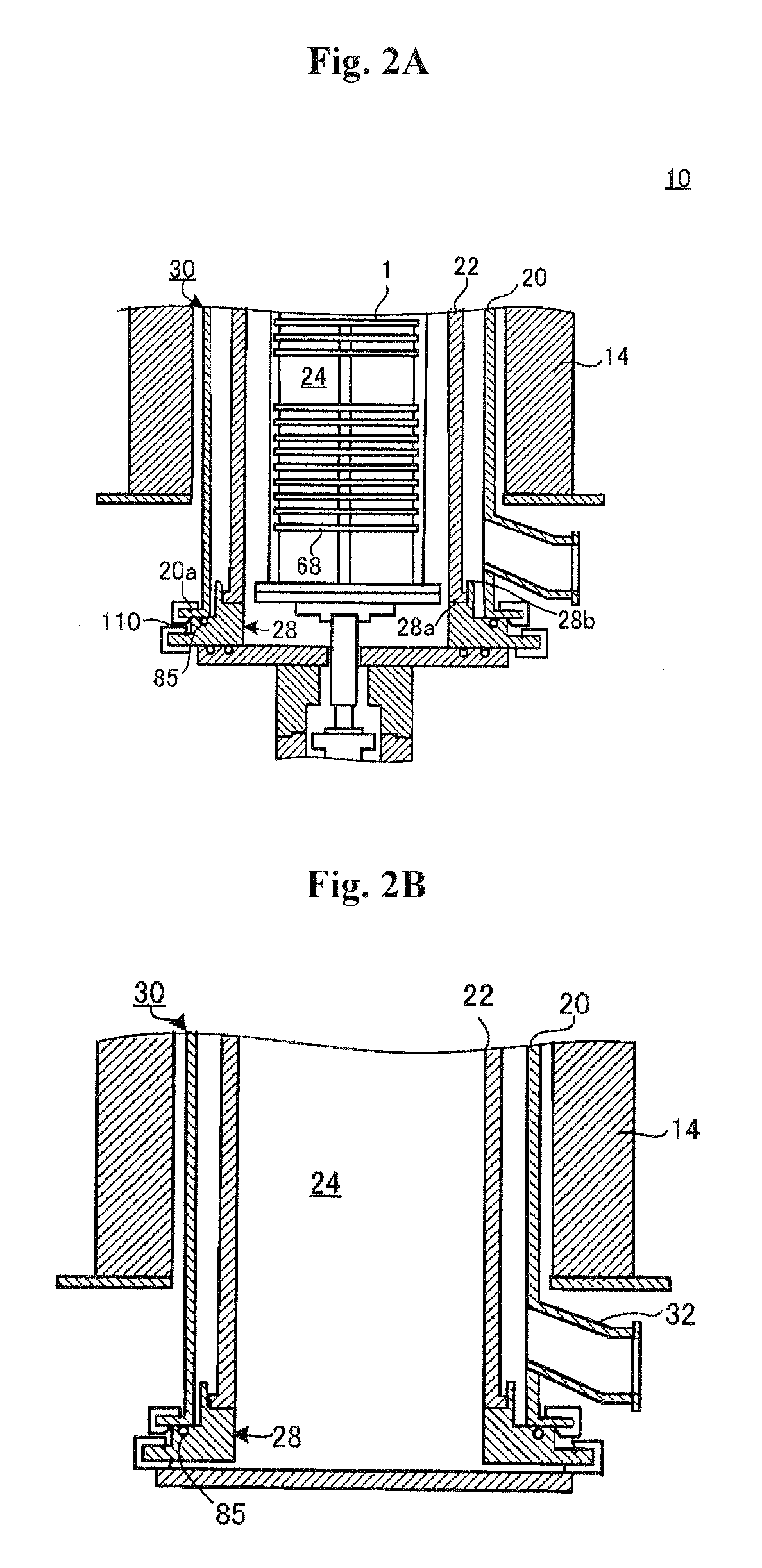
[0103]FIG. 7A and FIG. 7B illustrate an installation example of the heat insulation cylinder 90 in the present invention.
[0104]In the second embodiment, a lower cylinder part 90c is provided as a movement restriction member protruding downward from the outer periphery of the bottom surface 90a of the heat insulation cylinder 90 in a vertical direction. The lower cylinder part 90c of the heat insulation cylinder 90 is inserted into a groove 28d formed in the second placement part 28b of the manifold 28. Therefore, the horizontal movement and the oblique upward movement of the heat insulation cylinder 90 are suppressed. At the same time, since the horizontal movement of the inner tube 22 is suppressed by the lower cylinder part 90c of the heat insulation cylinder 90 and the groove 28d formed in the second placement part 28b, the oblique upward movement of the heat insulation cylinder 90 is also suppressed. Preferably, the relationship between the thickness A of the cylinder part 90c a...
third embodiment
[0106]In the present invention, as illustrated in FIG. 8, the height of the heat insulation cylinder 90 is set, from the top end to the bottom end of the heater 40, to be higher than the height of shielding the heating wire of the heating element, so that the heating wire of each heater 14, that is, the heating element, does not directly reach the third seal member 85. That is, the heat insulation cylinder 90 is set to be higher than the wire (heating wire) connecting the top end 14a of the heater 14 and the third seal member 85. In this manner, the temperature rise of the third seal member 85 is suppressed.
fourth embodiment
[0107]Herein, when the heat insulation cylinder 90 is provided, the temperature of the exhaust pipe 32 located at a position far from the center of the furnace becomes low and thus by-product may be adhered thereto. In the present invention, as illustrated in FIG. 9, a region facing the exhaust pipe 32 of the heat insulation cylinder 90 is notched upward to form a notch part 90d. Therefore, the heating wire of the heater 14 is partially received in the exhaust pipe 32, and the temperature of the exhaust pipe 32 partially rises. Hence, adhesion of by-product to the exhaust pipe 32 is prevented. Particularly, since the exhaust passage is curved at the lower part around an exhaust port inside the exhaust pipe 32, by-product is easily adhered. However, if the height of the bottom surface of the notch of the notch part 90d is set at the lower part around the exhaust port of the exhaust pipe 32 so high that the heating wire of the heater 14 directly arrives, adhesion of by-product is furt...
PUM
 Abstract
Description
Claims
Application Information