Formatter selectively outputting scan stimulus data from scan response data

a scan stimulus and data formatter technology, applied in the field of device scan testing, can solve the problem of increasing the cost of scan testers by 200 /b>

Active Publication Date: 2012-01-17
TEXAS INSTR INC
View PDF10 Cites 11 Cited by
  • Summary
  • Abstract
  • Description
  • Claims
  • Application Information

AI Technical Summary

Benefits of technology

[0009]This disclosure describes a method and apparatus for allowing the response data patterns from parallel scan paths of a circuit to be used to provide stimulus data patterns for input to the parallel scan paths of the circuit. Additionally, the response data patterns can provide expected data patterns for comparing against the response data patterns.

Problems solved by technology

The need for large high speed stimulus and expected data memories increases the cost of scan testers 200, which is reflected in the selling cost of the IC to the customer.

Method used


Image

  • Formatter selectively outputting scan stimulus data from scan response data
  • Formatter selectively outputting scan stimulus data from scan response data
  • Formatter selectively outputting scan stimulus data from scan response data

Examples


Embodiment Construction

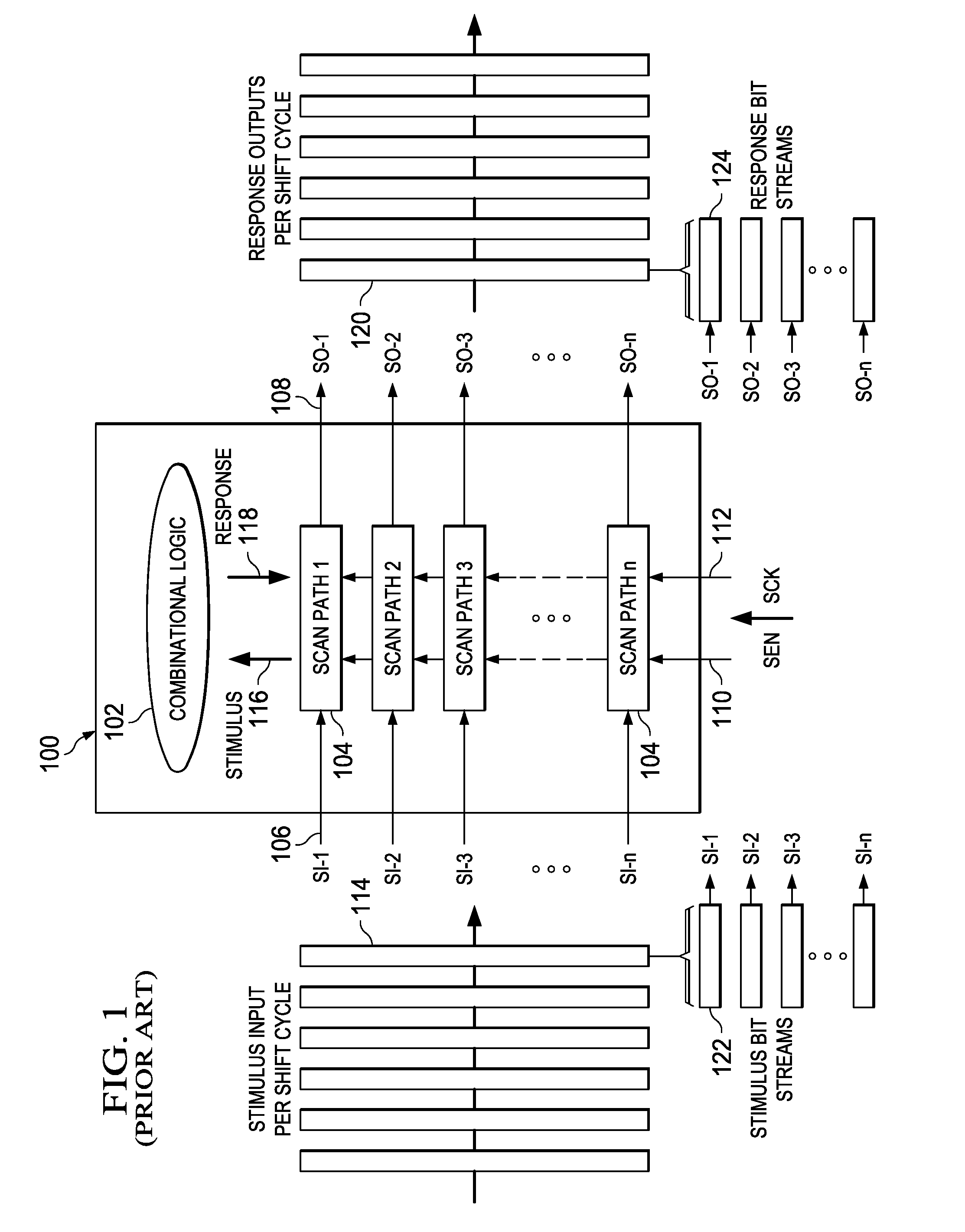
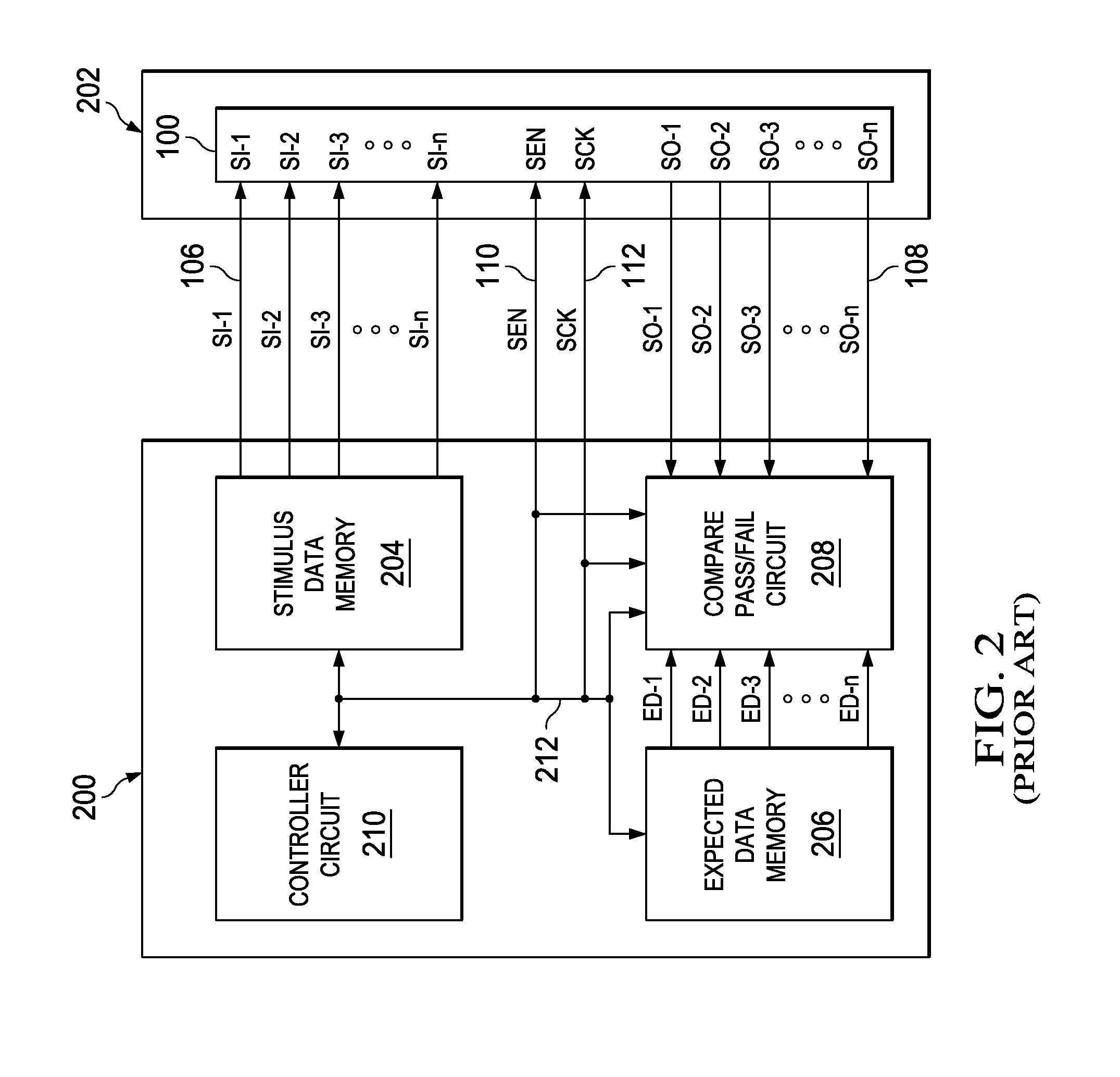
[0042]FIG. 3 illustrates an IC 304 containing a first embodiment of the disclosure coupled to a scan tester 300. The IC comprises an embedded circuit 301 to be scan tested and a formatter circuit 306. Circuit 301 is similar to circuit 100 of FIGS. 1 and 2 in that it has scan inputs (SI-1-n) 310, scan outputs (SO-1-n) 108, a SEN control input 110 and a SCK 112 control input. Circuit 301 differs from circuit 100 in that it includes a serial interface bus 307 consisting of a serial input (SI), serial mode input (SM), and a serial output (SO). The serial interface bus 307 of circuit 301 is controlled by bus 212 of tester 300. Circuit 301 receives SCK and SEN control inputs from the tester via bus 212 and outputs response data to the tester via SO-1-n 108 as previously described in regard to FIG. 2.

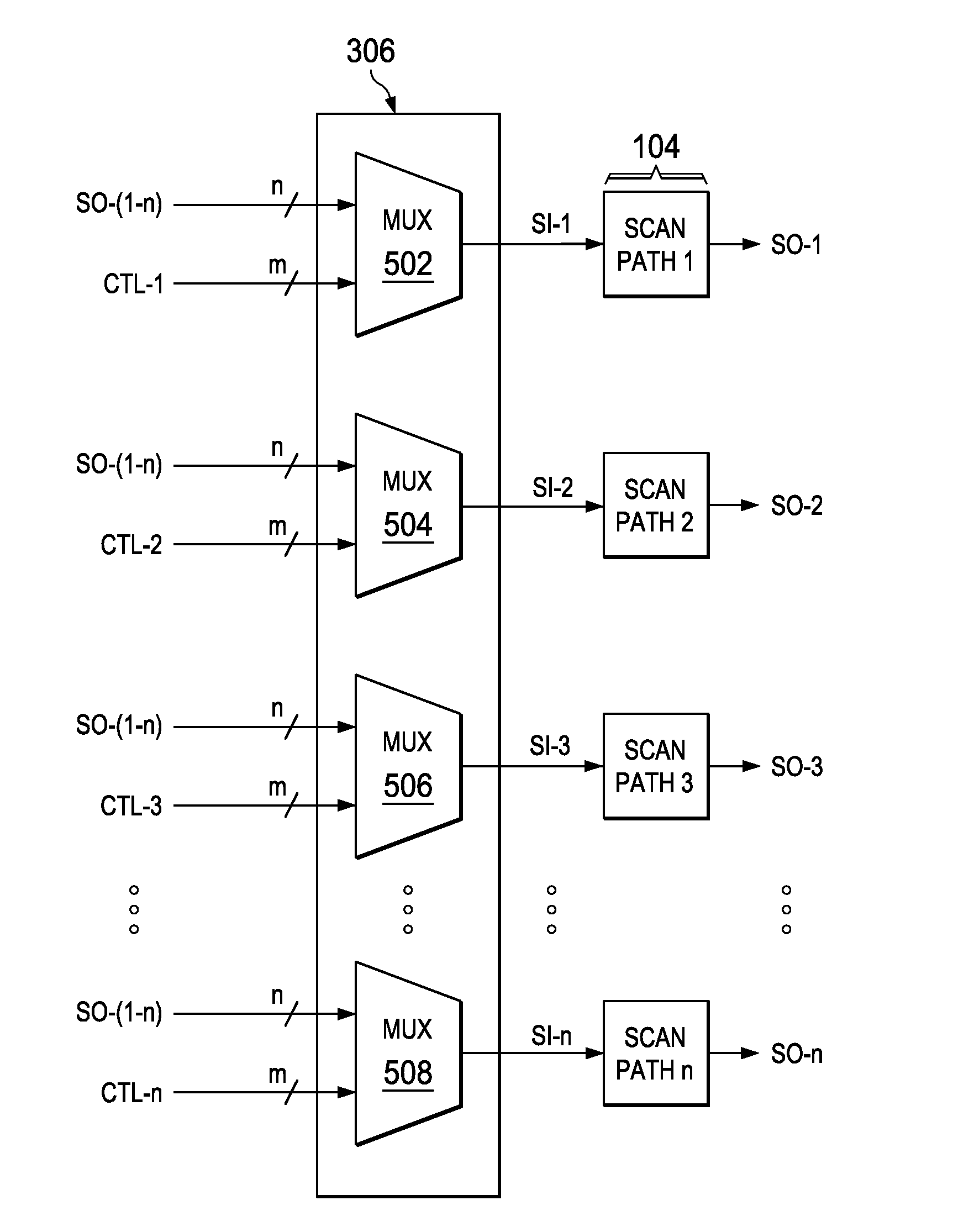
[0043]The formatter circuit 306, according to the disclosure, is used to provide the stimulus data patterns to circuit 301 via the SI-1-n inputs 310. The formatter 306 inputs response data pat...


PUM


Abstract

The disclosure describes a novel method and apparatus for allowing response data output from the scan outputs of a circuit under test to be formatted and applied as stimulus data input to the scan inputs of the circuit under test. Also the disclosure described a novel method and apparatus for allowing the response data output from the scan outputs of a circuit under test to be formatted and used as expected data to compare against the response data output from the circuit under test. Additional embodiments are also provided and described in the disclosure.

Description

CROSS REFERENCE TO RELATED PATENTS[0001]This application claims priority from Provisional Application No. 61 / 110,801, filed Nov. 3, 2008, currently pending.[0002]This application is related to application Ser. No. 08 / 931,791, filed Sep. 16, 1997, now U.S. Pat. No. 6,260,165, granted Jul. 10, 2001.FIELD OF THE DISCLOSURE[0003]This disclosure relates generally to device scan testing and in particular to device scan testing whereby the scan response outputs from a device under test are used for testing the device under test.BACKGROUND OF THE DISCLOSURE[0004]Most electrical circuits today, which may be IC devices or embedded sub-circuits within IC devices, are tested using parallel scan path approaches whereby the parallel scan paths are used to input and apply test stimulus patterns to a circuit's combinational logic and to capture and output test response patterns from the circuit's combinational logic.[0005]FIG. 1 illustrates a conventional example of a circuit's 100 combinational lo...

Claims


Application Information

Patent Timeline
Patent Type & Authority Patents(United States)
IPC IPC(8): G01R31/28
CPCG01R31/318536G01R31/3177G01R31/318544G01R31/31724G01R31/31725
Inventor WHETSEL, LEE D.
Owner TEXAS INSTR INC
Why Eureka
Try Eureka