Semiconductor device including through electrode and method of manufacturing the same

a technology of semiconductor devices and through electrodes, which is applied in the direction of semiconductor devices, semiconductor/solid-state device details, electrical apparatus, etc., can solve the problem of requiring some time to form through electrodes, and achieve the effect of reducing the amount of time required and suppressing the occurrence of voids

Inactive Publication Date: 2012-01-24
RENESAS ELECTRONICS CORP
View PDF15 Cites 6 Cited by
  • Summary
  • Abstract
  • Description
  • Claims
  • Application Information

AI Technical Summary

Benefits of technology

[0023]Accordingly, even in a case where a plating solution is frequently changed near the opening of the hole, the plating layer is not directly deposited on the opening portion of the hole. Thus, the opening portion of the hole can be prevented from being buried with the plating layer in a state where a void is formed inside the hole.
[0024]In addition, according to the present invention, since the seed layer is formed on the bottom surface of the hole and a part of the side wall of the hole, the plating layer can be formed fast as compared with a case where the seed layer is formed only on the bottom surface of the hole. Thereby, the amount of time required to form the through electrode can be reduced.
[0027]According to the present invention, a semiconductor device capable of suppressing the occurrence of a void in a through electrode and of reducing the amount of time required to form the through electrode, and a method of manufacturing the semiconductor device can be provided.

Problems solved by technology

Sho 63-127550, however, there is a problem that it requires some time to form a through electrode since the Au film 805 is formed only on the bottom surface of the through hole, and then the Au plating grows from the bottom to the top of the through hole to form the through electrode.

Method used


Image

  • Semiconductor device including through electrode and method of manufacturing the same
  • Semiconductor device including through electrode and method of manufacturing the same
  • Semiconductor device including through electrode and method of manufacturing the same

Examples


first embodiment

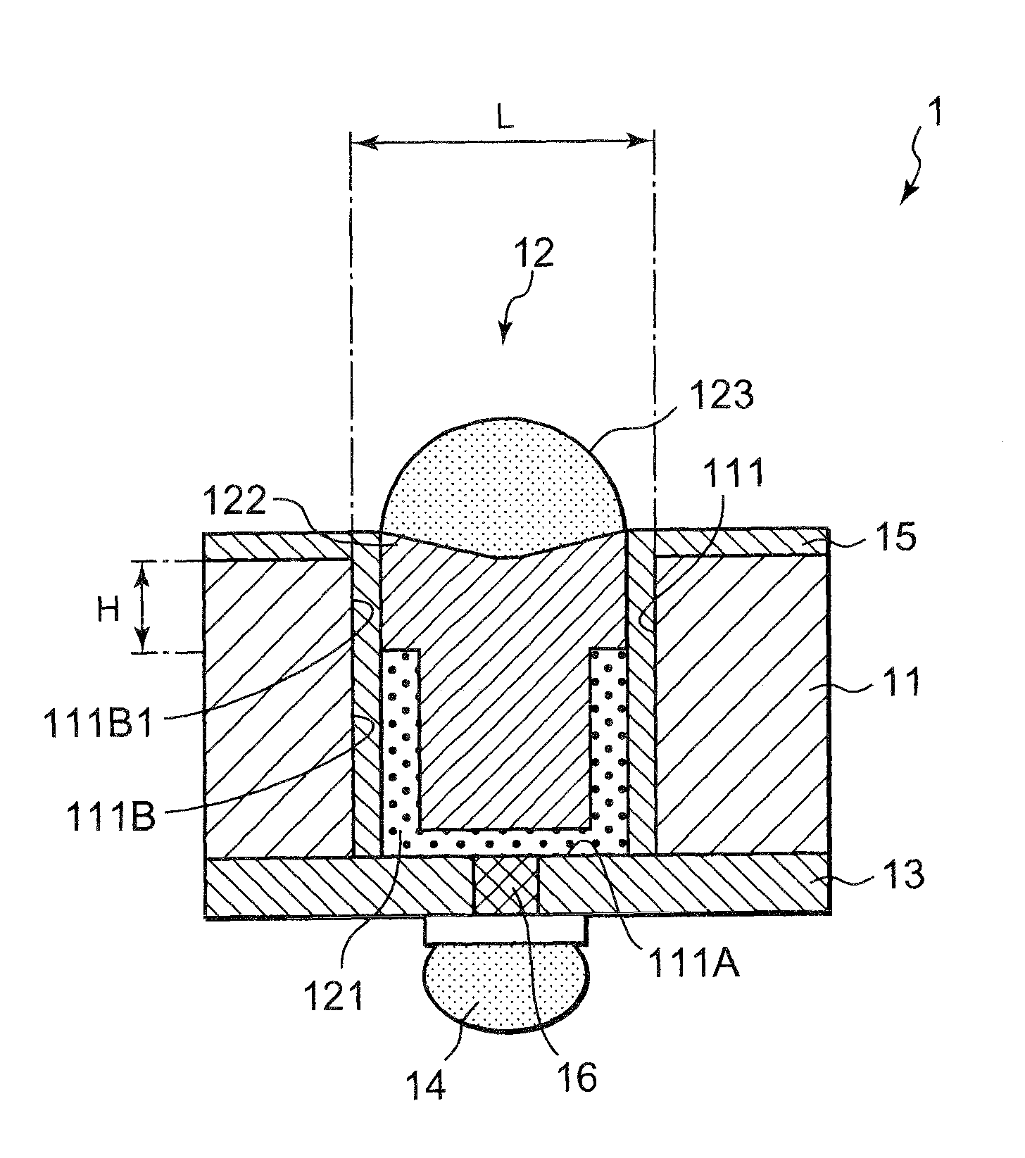
[0040]FIG. 1 shows a semiconductor device 1 according to the present embodiment.

[0041]First, outlines of the semiconductor device 1 according to the embodiment will be described. It should be noted that throughout the descriptions to be provided below, the same reference numerals are assigned to components that are identical to those having been described before, and descriptions thereof are omitted.

[0042]The semiconductor device 1 includes: a body 11, which is at least one of an insulating layer and a semiconductor layer each including a hole 111 formed therein; and a through electrode 12 provided in the hole 111 of the body 11.

[0043]The through electrode 12 includes a seed layer 121 and a plating layer 122.

[0044]The seed layer 121 covers a bottom surface 111A of the hole 111. On the other hand, the seed layer 121 does not cover a first region of a side wall 111B of the hole 111, the first region being a region from the opening of the hole 111 to a predetermined position between th...

second embodiment

[0111]A description will be given of a second embodiment of the present invention with reference to FIGS. 4A and 4B.

[0112]In the aforementioned embodiment, the diameter of the hole 111 of the semiconductor device 1 from the rear surface side of the semiconductor substrate 11 to the front surface side thereof is substantially constant, and thus, the shape of the hole 111 is a so-called straight shape.

[0113]In contrast to this, in the present embodiment, a side wall 211B of a hole 211 protrudes towards the outside of the hole 211 as shown in FIGS. 4A and 4B. The shape of the hole 211 is a so-called bowing shape. The side wall 211B of the hole 211 protrudes towards the outside of the hole 211 in an arched shape.

[0114]The diameter of hole 211 is substantially largest at the center portion of the hole 111 in the depth direction. The diameters of the respective openings on the front surface side and the rear surface side of the semiconductor substrate 11 are substantially the same.

[0115]T...

third embodiment

[0123]A description will be given of a third embodiment of the present invention with reference to FIG. 5.

[0124]In this embodiment, a plurality of grooves 311C each having a ring shape along the circumferential direction of a hole 311 are provided on a side wall 311B of the hole 311 of the semiconductor substrate 11.

[0125]In addition, although the seed layer 121 is provided on the side wall 111B of the hole 111 and the bottom surface 111A in a continuous manner in the first embodiment, and on the side wall 211B of the hole 211 and the bottom surface 111A in a continuous manner in the second embodiment, seed layers 321 in this embodiment are provided to the side wall 311B of the hole 311 in an intermittent manner. The other parts of the configuration in this embodiment are the same as those in the first embodiment.

[0126]A detailed description will be given below of a semiconductor device 3 according to the present embodiment.

[0127]As shown in FIG. 5D, the hole 311 of the semiconducto...


PUM


Abstract

The present invention provides a semiconductor device including at least one of an insulating layer and a semiconductor layer each including a hole formed therein, and a through electrode provided in the hole. In the semiconductor device, the side wall of the hole is constituted of a first region from the opening of the hole to a predetermined position between the opening of the hole and the bottom surface of the hole, and a second region from the predetermined position to the bottom surface of the hole. The through electrode includes a seed layer and a plating layer. The seed layer covers the second region and the bottom surface of the hole without covering the first region. In addition, the plating layer covers the seed layer and at least a part of the first region.

Description

BACKGROUND OF THE INVENTION[0001]1. Field of the Invention[0002]The present invention relates to a semiconductor device including a through electrode and a method of manufacturing the same.[0003]2. Description of Related Art[0004]In recent years, in order to achieve larger-scale integration of semiconductor devices, a three-dimensional mounting technique to stack semiconductor devices has been utilized. In order to adapt to such technique, it has been attempted to provide a through electrode in a semiconductor substrate.[0005]As a method of forming a through electrode, proposed is a method described in Japanese Laid-Open Patent Publication No. Sho 63-127550, for example.[0006]In this method, as shown in FIG. 1A, a source electrode 801 and an oxide film 802 are formed on the front surface (the lower surface in FIG. 10A) of a GaAs substrate 800, and mean while, a photoresist film 803 is formed on the rear surface (the upper surface in FIG. 10A) of the GaAs substrate 800.[0007]Next, a ...

Claims


Application Information

Patent Timeline
Patent Type & Authority Patents(United States)
IPC IPC(8): H01L23/52
CPCH01L21/76898H01L23/481H01L24/03H01L24/05H01L24/11H01L24/12H01L2224/0401H01L2224/1147H01L2224/11472H01L2224/11901H01L2224/13009H01L2224/13025H01L2224/13099H01L2224/131H01L2924/01004H01L2924/01005H01L2924/01013H01L2924/01014H01L2924/01022H01L2924/01027H01L2924/01028H01L2924/01029H01L2924/0103H01L2924/01046H01L2924/0105H01L2924/01073H01L2924/01074H01L2924/01078H01L2924/01079H01L2924/014H01L2924/04953H01L2924/10329H01L2924/00014H01L2924/01006H01L2924/01024H01L2924/01033H01L2224/05001H01L2224/0554H01L2224/06181H01L2224/14181
Inventor TAKAHASHI, NOBUAKIKOMURO, MASAHIROSOEJIMA, KOJIMATSUI, SATOSHIKAWANO, MASAYA
Owner RENESAS ELECTRONICS CORP
Why Eureka
Try Eureka