Image display medium and image formation device
a technology of image formation device and image display medium, which is applied in the direction of identification means, discharge tubes luminescnet screens, instruments, etc., can solve the problems of inability to display white, low contrast, and decreased image density, and achieve improved density contrast, enhanced hiding power, and improved tinting strength of second or first particles
- Summary
- Abstract
- Description
- Claims
- Application Information
AI Technical Summary
Benefits of technology
Problems solved by technology
Method used
Image
Examples
first embodiment
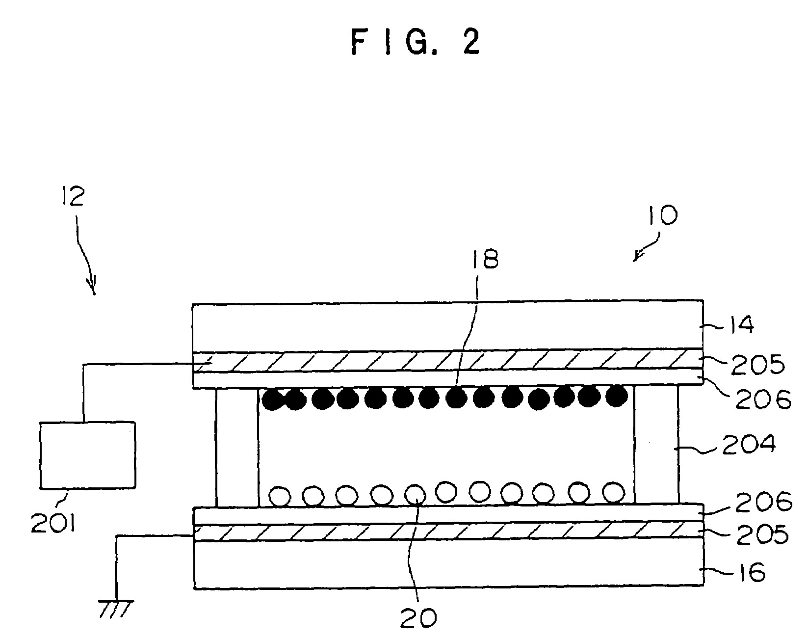
[0111]FIG. 2 is a diagram showing the schematic configuration of one example (the first embodiment) of the image formation device of the invention.
[0112]As shown in FIG. 2, an image formation device 12 according to the first embodiment has a voltage applying unit 201 as the generator. An image display medium 10 has a display substrate 14 on which an image is displayed, a non-display substrate 16 which faces the display substrate 14, a spacer 204 which is disposed between the display substrate 14 and the non-display substrate 16 and which seals the outer circumference between the two substrates, and black particles 18 and white particles 20 which are display particles and which are contained in space defined by the display substrate 14, the non-display substrate 16 and the spacer 204. Transparent electrodes 205 are disposed on each of opposing surfaces of the display substrate 14 and the non-display substrate 16, as described later. The transparent electrodes 205 disposed on the oppo...
second embodiment
[0118]Hereinafter, a second embodiment according to the invention will be explained in detail while referring drawings.
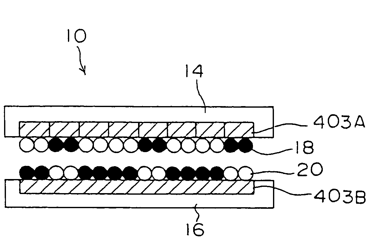
[0119]FIG. 3 is a diagram showing the schematic configuration of another example (the second embodiment) of the image formation device of the invention, and an image formation device which forms an image in an image display medium 10 by using a simple matrix driving method is shown.
[0120]Electrodes 403An and 404Bn (n is an integer) that control voltages in vertical and horizontal directions are arranged in the planar direction of the image display medium 10 including plural kinds of display particles (not shown) having different charging properties, so as to form a simple matrix structure. An electric field generator 405 has a waveform generator 405B and a power supply 405A, and the electrodes 403An are electrically connected to the power supply 405A. Another electric field generator 402 has a waveform generator 402B and a power supply 402A, and the electrodes 404Bn...
third embodiment
[0125]Hereinafter, a third embodiment of the invention will be described while referring drawings. FIG. 7 is a diagram showing the schematic configuration of another example (the third embodiment) of the image formation device of the invention, and specifically showing an image formation device with a printing electrode.
[0126]The image formation device 12 shown in FIG. 7 includes a printing electrode 11 and a counter electrode 26 which is opposite the printing electrode 11 and grounded.
[0127]The image display medium 10 can move in the direction of an arrow B between the printing electrode 11 and the counter electrode 26. The image display medium 10 includes a pair of substrates (the display substrate 14 and the non-display substrate 16) and the display particles 18 and 20 contained in space between the substrates. The image display medium moves in the direction of the arrow B such that the non-display substrate 16 be disposed in the vicinity of or brought into contact with the count...
PUM
| Property | Measurement | Unit |
|---|---|---|
| specific gravity | aaaaa | aaaaa |
| volume mean particle diameter | aaaaa | aaaaa |
| volume mean particle diameter | aaaaa | aaaaa |
Abstract
Description
Claims
Application Information


