Substrate processing method

a processing method and substrate technology, applied in the direction of basic electric elements, semiconductor/solid-state device manufacturing, electric devices, etc., can solve the problem of limiting the minimum size that can be mass produced using

Active Publication Date: 2012-01-31
TOKYO ELECTRON LTD
View PDF13 Cites 10 Cited by
  • Summary
  • Abstract
  • Description
  • Claims
  • Application Information

AI Technical Summary

Benefits of technology

[0009]Accordingly, in a first aspect of the present invention, there is provided a substrate processing method that processes a substrate in which a to-be-processed layer, an intermediate layer, and a mask layer are stacked in this order, and in which the mask layer has an opening to which part of the intermediate layer is exposed, comprising an opening width reducing step of accumulating deposit on a side wall surface of the opening in the mask layer using plasma produced from a deposition gas having a gas attachment coefficient S of 0.1 to 1.0, thus reducing an opening width of the opening.
[0051]The second aspect of the present invention can provide a substrate processing method comprising a to-be-processed layer etching step of transferring the opening in the intermediate layer corresponding to the opening in the mask layer reduced in opening width in the shrinking etching step onto the to-be-processed layer.

Problems solved by technology

However, the minimum size of a pattern in the photoresist film is determined by the minimum size that can be developed using photolithography, but there is a limit to the minimum size that can be mass produced using photolithography due to variations in focal length and so on.

Method used


Image

  • Substrate processing method
  • Substrate processing method
  • Substrate processing method

Examples


example 1

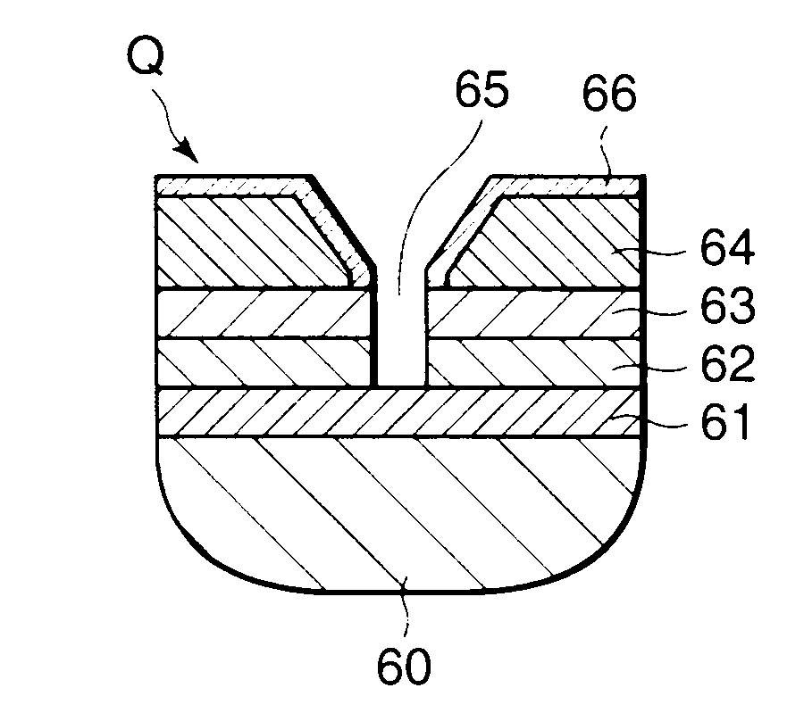
[0114]When a wafer Q in which intermediate layer and a photoresist film having an opening with an opening width of 60 nm are provided on a silicon base material was prepared, the pressure in the chamber was set to 1×10 Pa (75 mTorr), the temperature of the wafer Q was set to 50° C., CHF3 gas was supplied as a deposition gas into the chamber at a flow rate of 300 sccm, bias electrical power of 300 W was supplied to produce plasma, and shrinking processing was carried out in which the opening in the photoresist film was reduced, the thickness of deposit was 31 nm (opening width: 29 nm) 0.5 minute after the start of the processing, the thickness of deposit was 32 nm (opening width: 28 nm) 1 minute after the start of the processing, and the thickness of deposit was 33 nm (opening width: 27 nm) 3 minutes after the start of the processing.

[0115]It is clear from this result that the effect of reducing the opening width of the opening in the photoresist film in the shrinking processing reac...

example 16

[0147]A wafer Q having the photoresist film 64 whose initial opening width was 75 nm was subjected to the one-step approach processing using CHF3 gas as a deposition gas and CF3I gas as an anisotropic etching gas on the conditions that the flow ratio of the CHF3 gas to the CF3I gas was 4:1, the pressure in the chamber was 2×10 Pa (150 mTorr), the bias electrical power was 750+300 W, the temperature of the wafer Q was 60° C., and the shrinking amount and the etching states of the antireflective film 63 and the SiON film 62 were observed 30 seconds, 60 seconds, 120 seconds, 150 seconds, 180 seconds, and 300 seconds after the start of a test, and it was found that 30 seconds to 90 seconds after the start of the test, deposit (polymer) continuously accumulated on the side wall and the thickness of the deposit gradually increased while the antireflective film 63 was being punched. Moreover, until 90 seconds to 120 seconds after the start of the test, the shrinking further progressed, and...


PUM

PropertyMeasurementUnit
bias electrical poweraaaaaaaaaa
pressureaaaaaaaaaa
sizeaaaaaaaaaa

Abstract

A substrate processing method that forms an opening, which has a size that fills the need for downsizing a semiconductor device and is to be transferred to an amorphous carbon film, in a photoresist film of a substrate to be processed. Deposit is accumulated on a side wall surface of the opening in the photoresist film using plasma produced from a deposition gas having a gas attachment coefficient S of 0.1 to 1.0 so as to reduce the opening width of the opening.

Description

BACKGROUND OF THE INVENTION[0001]1. Field of the Invention[0002]The present invention relates to a substrate processing method, and in particular to a substrate processing method that carries out processing on a substrate in which a to-be-processed layer, an intermediate layer, and a mask layer are stacked in this order.[0003]2. Description of the Related Art[0004]There has been known a wafer for a semiconductor device in which an oxide film containing impurities such as a TEOS (tetra ethyl ortho silicate) film, a conductive film such as a TiN film, an antireflective film (BARC film), and a photoresist film formed through CVD processing or the like are stacked in this order on a silicon base material (see, for example, Japanese Laid-open Patent Publication (Kokai) No. 2006-190939). The photoresist film is formed to have a predetermined pattern by photolithography and acts as a mask when the antireflective film and the conductive film are etched.[0005]In recent years, as semiconducto...

Claims


Application Information

Patent Timeline
Patent Type & Authority Patents(United States)
IPC IPC(8): H01L21/311
CPCH01L21/0212H01L21/02274H01L21/0337H01L21/0338H01L21/31116H01L21/31122H01L21/31138H01L21/31144H01L21/3127H01L21/0271
Inventor HONDA, MASANOBUICHIKAWA, HIRONOBU
Owner TOKYO ELECTRON LTD
Why Eureka
Try Eureka