
Active device array substrate, color filter substrate and manufacturing methods thereof

a technology of active devices and array substrates, which is applied in the direction of coatings, optical elements, instruments, etc., can solve the problems of affecting common pastes on color filter substrates or active device array substrates may form poor electrical contact with counter substrates, and the coating technique cannot produce alignment material layers with a high degree of film surface accuracy. achieve the effect of improving the displaying quality of liquid crystal display panels

Active Publication Date: 2012-02-21
AU OPTRONICS CORP
View PDF6 Cites 5 Cited by
  • Summary
  • Abstract
  • Description
  • Claims
  • Application Information

AI Technical Summary

Benefits of technology

[0008]Accordingly, one objective of the present invention is to provide an active device array substrate capable of improving the displaying quality of a liquid crystal display panel.
[0009]Another objective of the present invention is to provide a color filter substrate capable of improving the displaying quality of a liquid crystal display panel.
[0036]In the active device array substrate or color filter substrate, according to one embodiment of the present invention, the partition configuration restricts the region for forming the alignment material layer so that the alignment material layer does not cover the common paste. After assembling the active device array substrate or the color filter substrate with a counter substrate to form a liquid crystal display panel, the circuit on the active device array substrate or color filter substrate can electrically conduct with the circuit on the counter substrate through the common paste. Therefore, the liquid crystal display panel has better displaying quality. In other words, the active device array substrate or color filter substrate is able to improve the displaying quality of the liquid crystal display panel. In addition, the method of fabricating the active device array substrate or the method of fabricating the color filter substrate according to the present invention also includes the fabrication of a partition configuration. Through the partition configuration, the region for forming the alignment material layer is controlled to prevent the alignment material layer from covering the common paste.

Problems solved by technology

However, as the dimension of a substrate increases, the coating technique can no longer produce an alignment material layer with a high degree of film surface accuracy.
In the process of using the ink-jet printing method to form the alignment material layer, part of the alignment material layer may cover the common paste due to the difficulty of controlling the diffusion of alignment material near the edges.
Therefore, after assembling the color filter substrate or the active device array substrate having an alignment material layer formed by the ink-jet printing method with a counter substrate to form a liquid crystal display panel, the common paste on the color filter substrate or the active device array substrate may form a poor electrically contact with the corresponding common paste on the counter substrate.
Ultimately, the displaying quality of the liquid crystal display panel is affected.

Method used


Image

  • Active device array substrate, color filter substrate and manufacturing methods thereof
  • Active device array substrate, color filter substrate and manufacturing methods thereof
  • Active device array substrate, color filter substrate and manufacturing methods thereof

Examples


Embodiment Construction

[0047]Reference will now be made in detail to the present preferred embodiments of the invention, examples of which are illustrated in the accompanying drawings. Wherever possible, the same reference numbers are used in the drawings and the description to refer to the same or like parts.

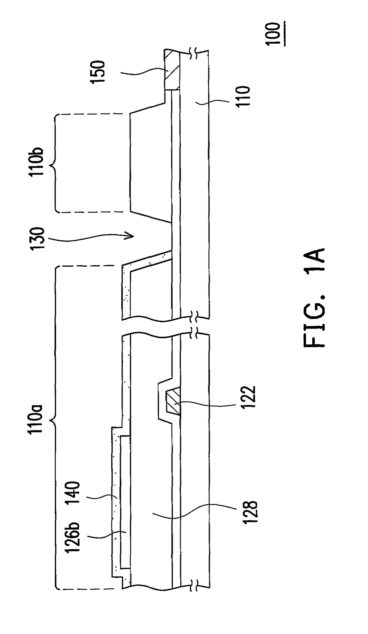
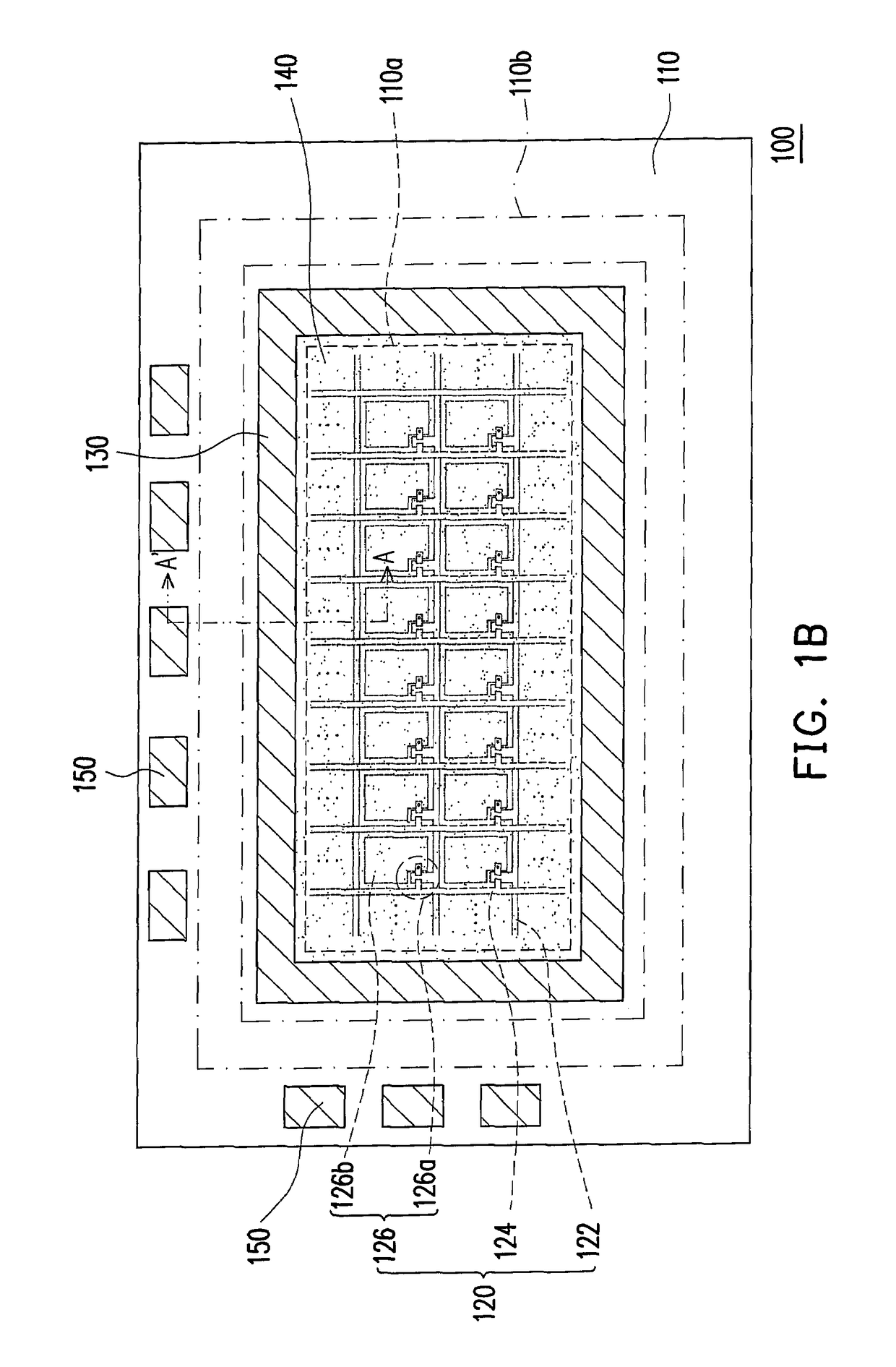
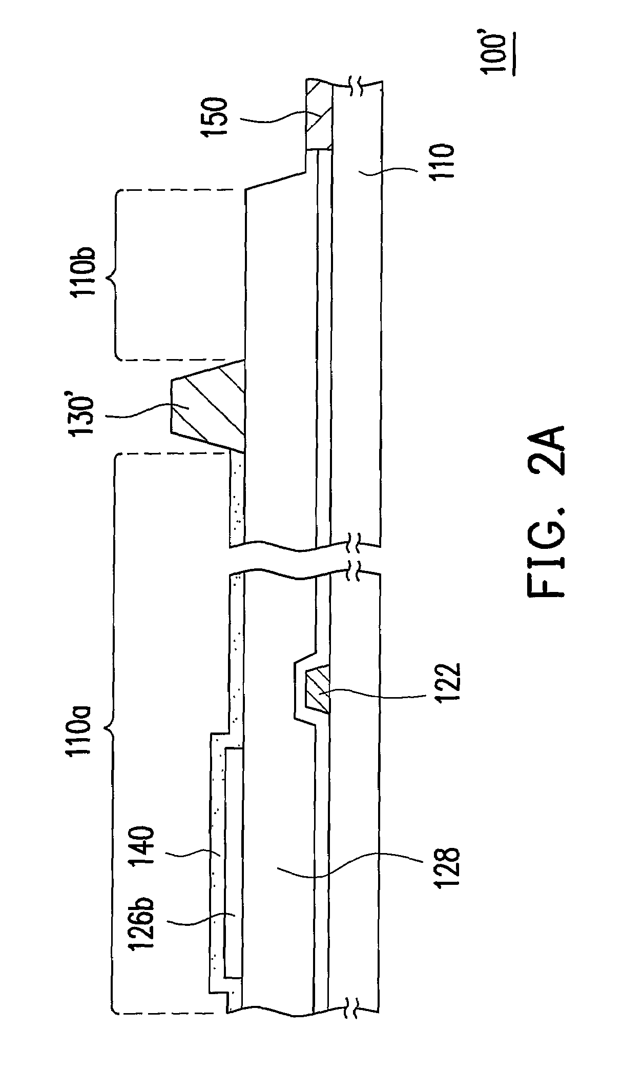
[0048]FIG. 1A is a schematic cross-sectional view showing the structure of an active device array substrate according to one embodiment of the present invention. FIG. 1B is a top view of the active device array substrate in FIG. 1A. In fact, FIG. 1A is a cross-sectional view along line A-A′ of FIG. 1B. As shown in FIGS. 1A and 1B, the active device array substrate 100 includes a substrate 110, a pixel array 120, a partition configuration 130 and an alignment material layer 140. The substrate 110 is, for example, a glass substrate, a quartz substrate, or other substrate made of a suitable material. The substrate 110 has an alignment region 110a and a predetermined sealing region 110b. The predetermine...


PUM

PropertyMeasurementUnit
widthaaaaaaaaaa
widthaaaaaaaaaa
distanceaaaaaaaaaa

Abstract

An active device array substrate comprising a substrate, a pixel array, a partition configuration and an alignment material layer is provided. The substrate has an alignment region and a predetermined sealing region. The predetermined sealing region surrounds the alignment region. The pixel array is disposed on the substrate within the alignment region. The partition configuration is disposed on the substrate between the predetermined sealing region and the alignment region. The alignment material layer is disposed within the alignment region and covers the pixel array.

Description

CROSS-REFERENCE TO RELATED APPLICATION[0001]This application claims the priority benefit of Taiwan application serial no. 95114669, filed Apr. 25, 2006. All disclosure of the Taiwan application is incorporated herein by reference.BACKGROUND OF THE INVENTION[0002]1. Field of the Invention[0003]The present invention relates to an active device array substrate, a color filter substrate and manufacturing methods thereof. More particularly, the present invention relates to an active device array substrate and a color filter substrate each having a partition configuration and methods of manufacturing the active device array substrate and the color filter substrate each having a partition configuration.[0004]2. Description of Related Art[0005]The popularity of multimedia in our society came as a result of the rapid advancement in the fabrication of semiconductor devices and display apparatuses. In particular, liquid crystal displays, with the advantages of high displaying quality, good spa...

Claims


Application Information

Patent Timeline
Patent Type & Authority Patents(United States)
IPC IPC(8): H01L29/10
CPCG02F1/133711B05D5/065G02B5/22H01L33/58G02F1/1339
Inventor TUNG, YUAN-HUNGLEE, YI-WEI
Owner AU OPTRONICS CORP
Learn More