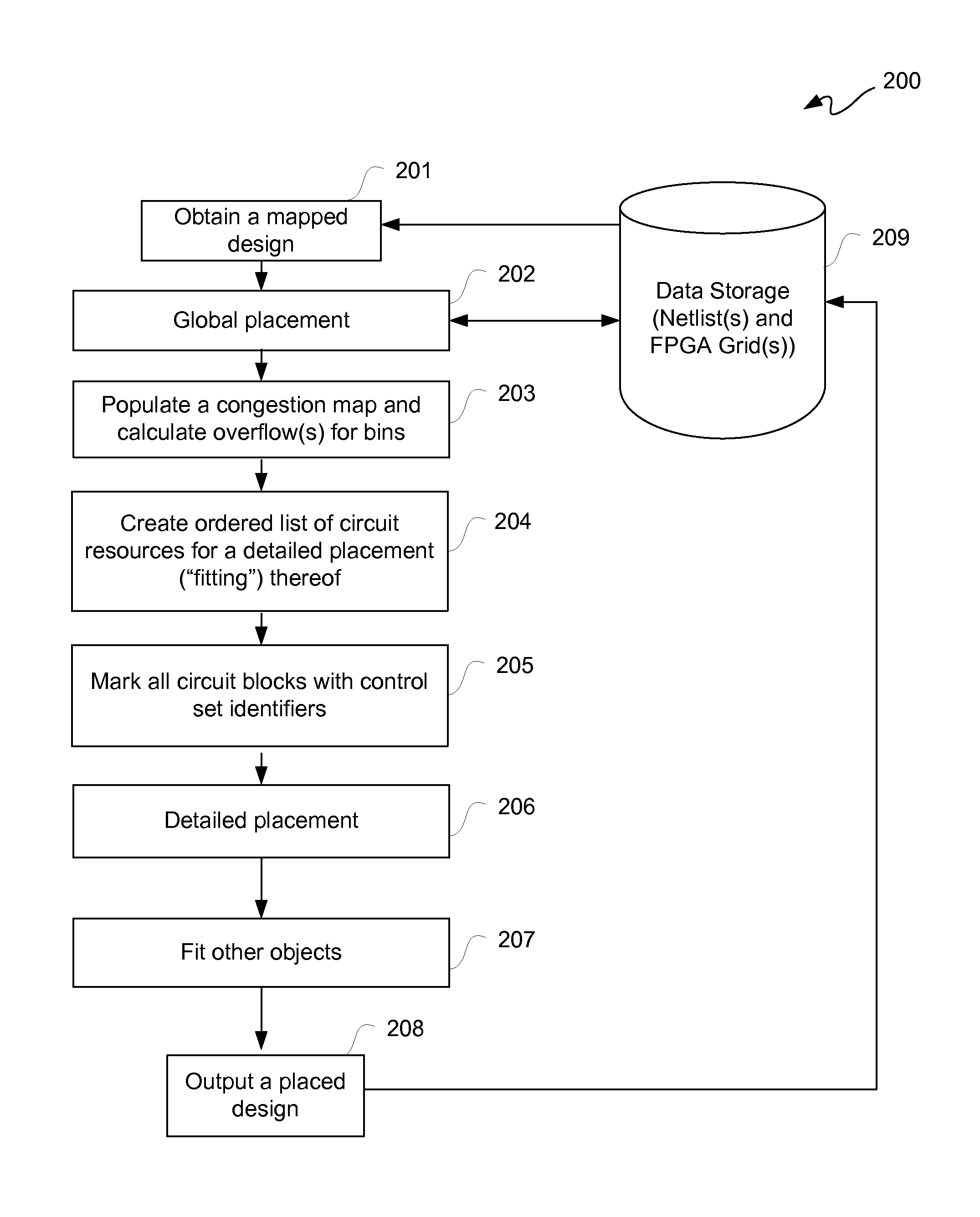
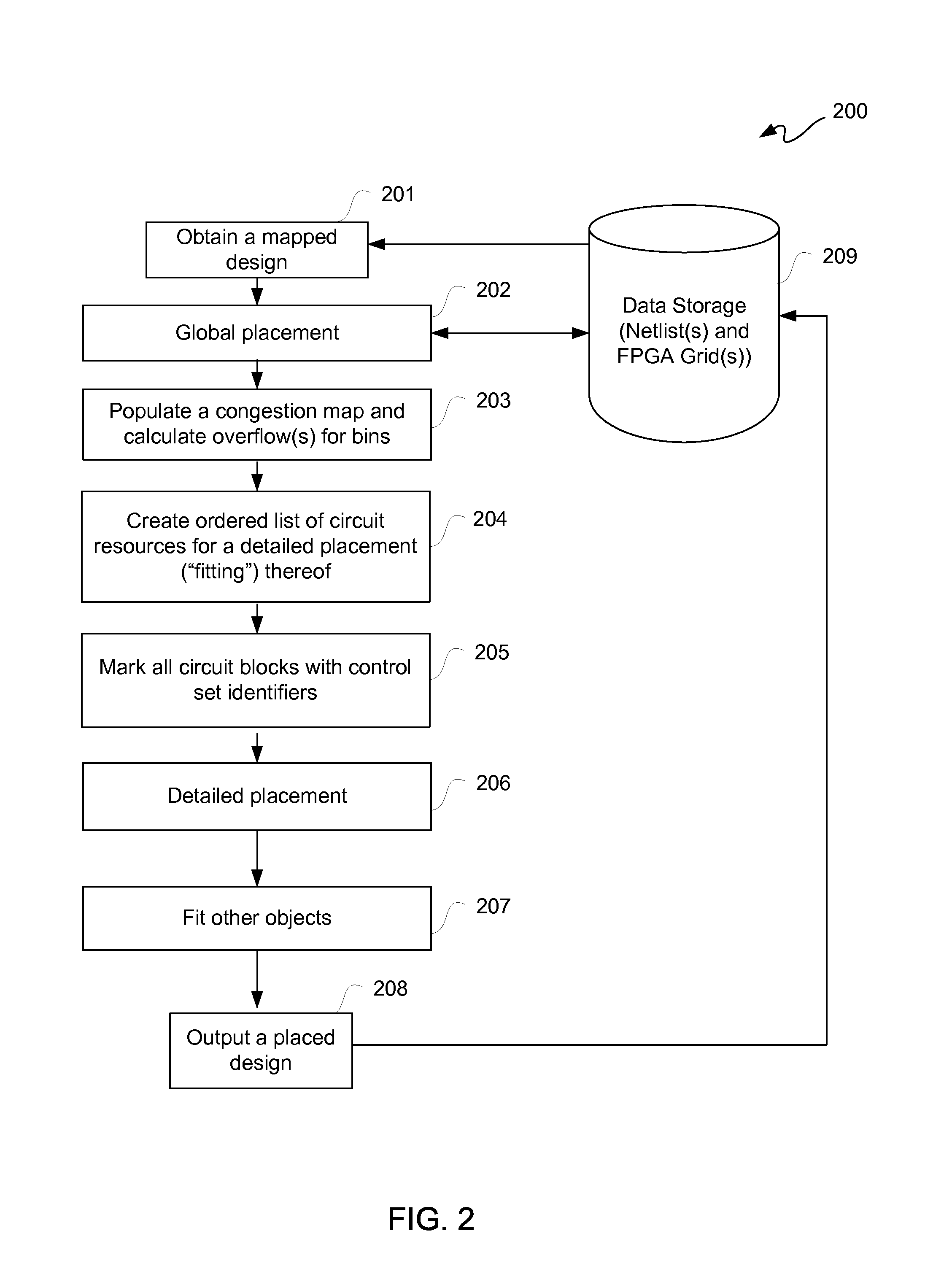
[0017]In one or more other embodiments of a method for fitting a circuit design having been synthesized, one or more of the following aspects may be included. The method may further comprise repeating the selecting, the locating, the acquiring, the categorizing, and the placing for each of the sequential circuit objects on the list to complete the second placement. The statuses may include categories of control set identifiers and an unused category. The categorizing of the nearest neighbor circuit resource blocks may include labeling the nearest neighbor circuit resource blocks as one of identical to the first control set identifier, related to the first control set identifier, incompatible with the first control set identifier, or unused. The method may further comprise sorting the overflow conditions of the circuit resource blocks used in the first placement from most overflowing to least overflowing to provide the list and initiating the second placement by selection of the first circuit object in association with the first circuit resource block, wherein the first circuit resource block is the most overflowing. The method may further comprise sorting the sequential circuit objects according to size and timing to provide the list.
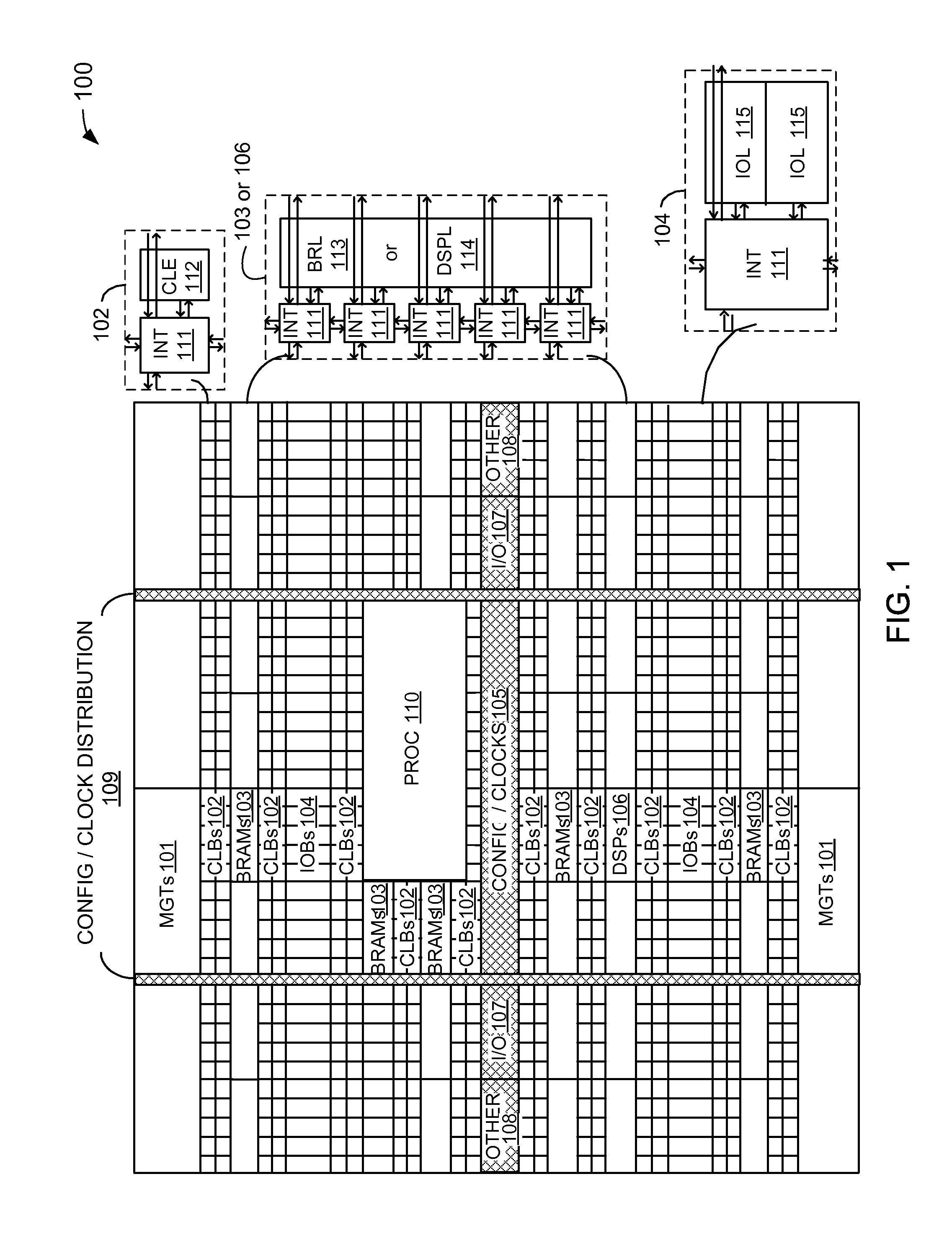
[0018]The sequential circuit objects may be sized responsive to number of objects in associated relationally placed macros. The first placement may be a global placement; and the second placement may be a detailed placement. The sequential circuit objects may include registers. The acquiring of the nearest neighbor circuit resource blocks of the first circuit resource block may include: snapping the first circuit object to the site; the site being associated with a grid of the circuit resource blocks; and performing a first spiral search to acquire the nearest neighbor circuit resource blocks of the first circuit resource block. The integrated circuit may be a Field Programmable Gate Array (“FPGA”), and the grid may be an FPGA grid of the circuit resource blocks. The sequential circuit objects may represent clocked flip-flops and look-up table random access memories. The acquiring of the nearest neighbor circuit resource blocks of the first circuit resource block may be for a portion of the congestion map responsive to a scalable window. The integrated circuit may be a Field Programmable Gate Array (“FPGA”); the grid may be an FPGA grid of the circuit resource blocks; the scalable window may be for selection of a portion of the FPGA grid; and the scalable window may have a granularity of at least one slice per bin of the congestion map. The placing of the first circuit object in the nearest neighbor of the nearest neighbor circuit resource blocks of the first circuit resource block may be favored over placement in another of the nearest neighbor circuit resource blocks having a higher priority but with an unused status.
[0019]The method may further comprise: selecting a second circuit object from the list of the sequential circuit objects; the second circuit object associated with a second control set identifier different from the first control set identifier; locating another site for placement of the second circuit object; the other site being associated with a second circuit resource block; the second circuit resource block being associated with the circuit resource blocks of the integrated circuit; acquiring nearest neighbor circuit resource blocks with respect to the second circuit resource block; categorizing the nearest neighbor circuit resource blocks of the second circuit resource block responsive to statuses thereof; placing the second circuit object in a nearest neighbor of the nearest neighbor circuit resource blocks of the second circuit resource block having the unused status for the second placement; the nearest neighbor having associated therewith another categorization from the categorizing including the second control set identifier of the second circuit object; the first control set identifier and the second control set identifier being related wherein the first circuit object and the second circuit object are capable of being resynthesized for placement of the second circuit object in the first circuit object; and the placing of the second circuit object in the nearest neighbor of the nearest neighbor circuit resource blocks of the second circuit resource block is favored over yet another of the nearest neighbor circuit resource blocks having another higher priority with a compatible status.
[0020]In another embodiment of a method for fitting a circuit design having been synthesized, a machine-readable medium has stored thereon information representing instructions that, when executed by a processor, cause the processor to perform operations comprising: obtaining a mapped design for a circuit design; performing a first placement of the mapped design in association with an integrated circuit; generating a congestion map responsive to the first placement; identifying overflow conditions in the congestion map; creating a list of sequential circuit objects for a second placement responsive at least in part to the overflow conditions identified; marking circuit blocks associated with the integrated circuit with control set identifiers; selecting a first circuit object from the list of the sequential circuit objects, wherein the first circuit object is associated with a first control set identifier; locating a site for placement of the first circuit object, wherein the site is associated with a first circuit resource block, and the first circuit resource block is associated with circuit resource blocks of the integrated circuit; acquiring nearest neighbor circuit resource blocks with respect to the first circuit resource block; categorizing the nearest neighbor circuit resource blocks of the first circuit resource block in response to statuses; and placing, with a placer operative with the processor, the first circuit object in a nearest neighbor of the nearest neighbor circuit resource blocks of the first circuit resource block for a second placement, wherein the nearest neighbor is associated with a categorization from the act of categorizing including the first control set identifier of the first circuit object.
[0021]In yet another embodiment of a method for fitting a circuit design having been synthesized, the method includes steps of: obtaining a mapped design for the circuit design; performing a first placement of the mapped design in association with an integrated circuit; marking circuit blocks associated with the integrated circuit with control set identifiers; selecting a first circuit object from a list of the sequential circuit objects; the first circuit object associated with a first control set identifier; locating a site for placement of the first circuit object; the site being associated with a first circuit resource block; the first circuit resource block being associated with circuit resource blocks of the integrated circuit; acquiring nearest neighbor circuit resource blocks with respect to the first circuit resource block; categorizing the nearest neighbor circuit resource blocks of the first circuit resource block in response to statuses; placing with a placer operating in a computer the first circuit object in a nearest neighbor of the nearest neighbor circuit resource blocks of the first circuit resource block for a second placement; and the nearest neighbor having associated therewith a categorization from the categorizing including the first control set identifier of the first circuit object.
[0022]In one or more other embodiments of a method for fitting a circuit design having been synthesized, one or more of the following steps may be included: generating a congestion map responsive to the first placement; identifying overflow conditions in the congestion map; creating a list of sequential circuit objects for the second placement responsive at least in part to the overflow conditions identified, where the overflow conditions calculated with a processor of the computer; and repeating the selecting, the locating, the acquiring, the categorizing, and the placing for each of the sequential circuit objects on the list to complete the second placement. The statuses may include categories of control set identifiers and an unused category; and the categorizing of the nearest neighbor circuit resource blocks includes labeling the nearest neighbor circuit resource blocks as one of identical to the first control set identifier, related to the first control set identifier, incompatible with the first control set identifier, or unused.


