Supercharge Your Innovation With Domain-Expert AI Agents!

Method for packaging a sensor unit

a sensor unit and packaging technology, applied in the direction of measuring apparatus components, instruments, electric discharge lamps, etc., can solve the problems of high complexity of manufacturing processes and structures, inability to control glues, and inability to fix metal frames in a manner that is not suitable for compactness and repair, so as to improve isolation effectiveness, reduce mold cost, and improve reliability

Inactive Publication Date: 2012-04-03
LITE ON SINGAPORE PTE LTD
View PDF2 Cites 3 Cited by
  • Summary
  • Abstract
  • Description
  • Claims
  • Application Information

AI Technical Summary

Benefits of technology

The method enhances signal isolation effectiveness, improves reliability, and reduces manufacturing costs by using a single mold for both packaging steps, ensuring precise assembly and minimizing the separation issues of packaging components.

Problems solved by technology

However, the final packaging structure must generally form locking structures to properly assemble the metal frame.
The manufacturing processes and the structures are highly complex.
The glues are not easily controlled.
On the other hand, the metal frame will not be fixed properly or in an acceptably compact manner with the packaging structure if the amount of glue used is not sufficient.
In the case that the metal frame shifts or moves relative to the packaging structure, or departs from the packaging structure, the signals cannot be precisely isolated and shielded.
Thus, the assembling processes are more and more complex, thereby complicating assembly processes and the manufacturing yields are likely to decline.

Method used


Image

  • Method for packaging a sensor unit
  • Method for packaging a sensor unit
  • Method for packaging a sensor unit

Examples


Embodiment Construction

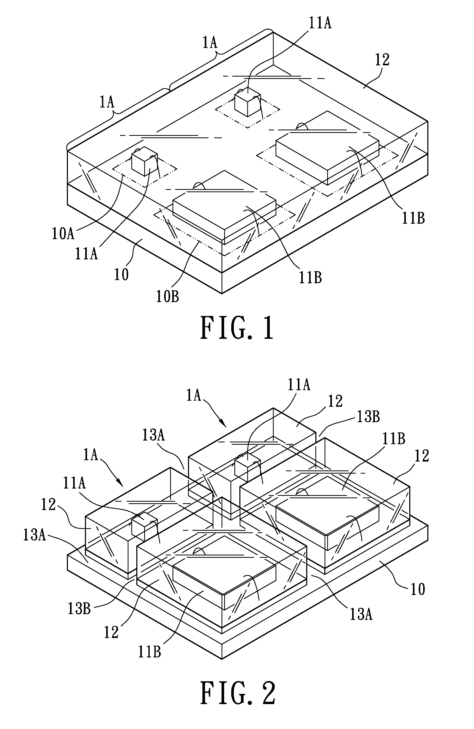
[0028]Please refer to FIGS. 1 to 4; the present invention provides a packaging method of a sensor unit 1. Two molding steps of one single mold are provided in the packaging method to package and to isolate the elements of the sensor unit 1. The manufacturing cost is decreased and the assembling problems of the traditional sensor are further resolved. The packaging method has the following steps.

[0029]Step 1 of the present invention is providing a substrate 10 having a plurality of sensor unit area 1A thereon. As shown in FIG. 1, the substrate 10 of the first embodiment has two sensor unit areas 1A and each sensor unit area 1A can be manufactured as one single sensor unit 1 (as shown in FIG. 4). Each sensor unit area 1A is partitioned into two individual circuit areas 10A, 10B (or more than two circuit areas). The two circuit areas 10A, 10B are formed on a surface of the substrate 10 and in the interior of the substrate 10, there is a signal-emitting device 11A of the sensor unit 1 a...


PUM

PropertyMeasurementUnit
distanceaaaaaaaaaa
depthaaaaaaaaaa
widthaaaaaaaaaa

Abstract

A method for packaging the sensor units is shown below. First step is providing a substrate, and each sensor area on the substrate is partitioned into two individual circuit areas. An emitter and a detector are installed on the two circuit areas respectively. Step two is forming a first packaging structure to cover the two circuit areas, the emitter and the detector by a mold. Next step is cutting the first packaging structure to form cut groove between and around the emitter and the detector. Next step is forming a second packaging structure in the cut grooves by the same mold. At last, the panel of sensor units is diced and separated as individual sensor units. As above-mentioned, the second packaging structure is used for isolating the signals of the emitter and the detector.

Description

BACKGROUND OF THE INVENTION[0001]1. Field of the Invention[0002]The present invention relates to a sensor unit and a method for packaging the sensor unit, in particular to a packaging method with two molding steps using one mold and a sensor unit with high precision and high reliability.[0003]2. Description of Related Art[0004]Depending on the design of the electronic product, the electronic product is controlled by the input devices such as a key, a keypad, a tracking ball, or a touch panel screen. Recently, the touch panel screen has been widely used in electronic applications. The touch panel screen includes a touch panel which has a transparent panel with a sensitive surface to cover the displaying area of the screen. Users can select the items or move the cursor by using a finger or a touch pen on the touch panel screen so that the electronic device is controlled by the touch signals from the touch panel screen. For example, an IR proximity sensor is widely used in mobile commu...

Claims


Application Information

Patent Timeline
Patent Type & Authority Patents(United States)
IPC IPC(8): H01K3/22
CPCG01D11/245Y10T29/49158Y10T29/49176Y10T29/49172Y10T29/4916H01L2224/48227H01L2224/97
Inventor LIM, SIN-HENGGE, AMY
Owner LITE ON SINGAPORE PTE LTD
Features
  • R&D
  • Intellectual Property
  • Life Sciences
  • Materials
  • Tech Scout
  • Unparalleled Data Quality
  • Higher Quality Content
  • 60% Fewer Hallucinations
Learn More