
Wiring structure of liquid crystal display device and liquid crystal display device

a liquid crystal display device and wiring structure technology, applied in static indicating devices, non-linear optics, instruments, etc., can solve the problems of limited area inside liquid crystal display devices, and difficulty for workers to distinguish wirings around the edges of display panels, etc., to avoid abnormal display quality of liquid crystal display devices. easy to know

Inactive Publication Date: 2012-05-08
CHUNGHWA PICTURE TUBES LTD
View PDF2 Cites 0 Cited by
  • Summary
  • Abstract
  • Description
  • Claims
  • Application Information

AI Technical Summary

Benefits of technology

"The present invention provides a wiring structure for a liquid crystal display device that is easy to view and distinguish before and after cutting and polishing. The wiring structure includes a substrate, electrical elements, and wirings. The outermost peripheral wiring has a different pattern from the inner wirings, which helps to easily identify any changes in the wiring patterns after cutting and polishing. This prevents abnormal display quality and ensures good quality of the liquid crystal display device."

Problems solved by technology

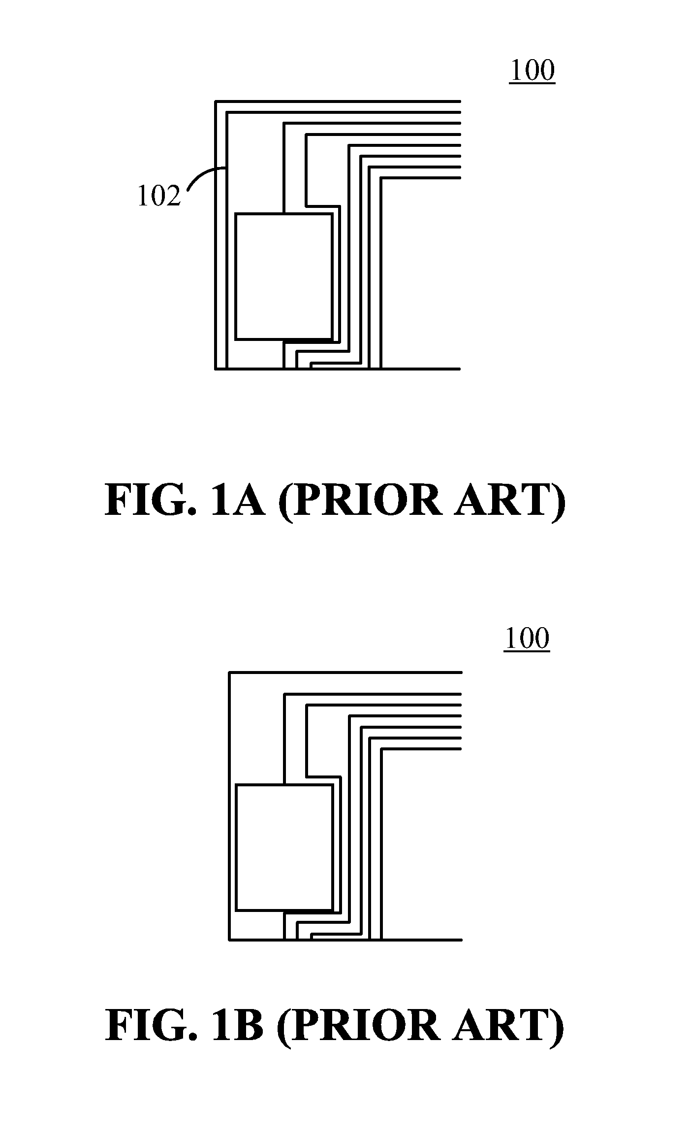
However, because the areas inside the liquid crystal display device are limited, the wirings are often closer to the edges being cut and polished.
The wirings around the edges of the display panel still remain a straight-line pattern before and after the edges of the display panel are polished, so it is difficult for the workers to distinguish a border of the wirings around the edges of the display panel.
Resistance of the wiring areas is accordingly changed to affect output signals, and display quality of the liquid crystal display device 100 is thus abnormal.
The above-mentioned problem affects the output signals and leads to the abnormal display quality of the liquid crystal display device.

Method used


Image

  • Wiring structure of liquid crystal display device and liquid crystal display device
  • Wiring structure of liquid crystal display device and liquid crystal display device
  • Wiring structure of liquid crystal display device and liquid crystal display device

Examples


Embodiment Construction

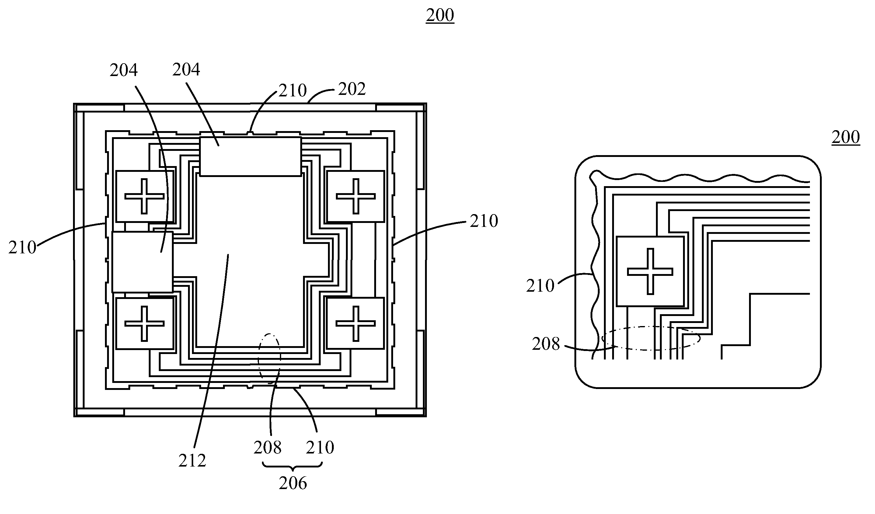
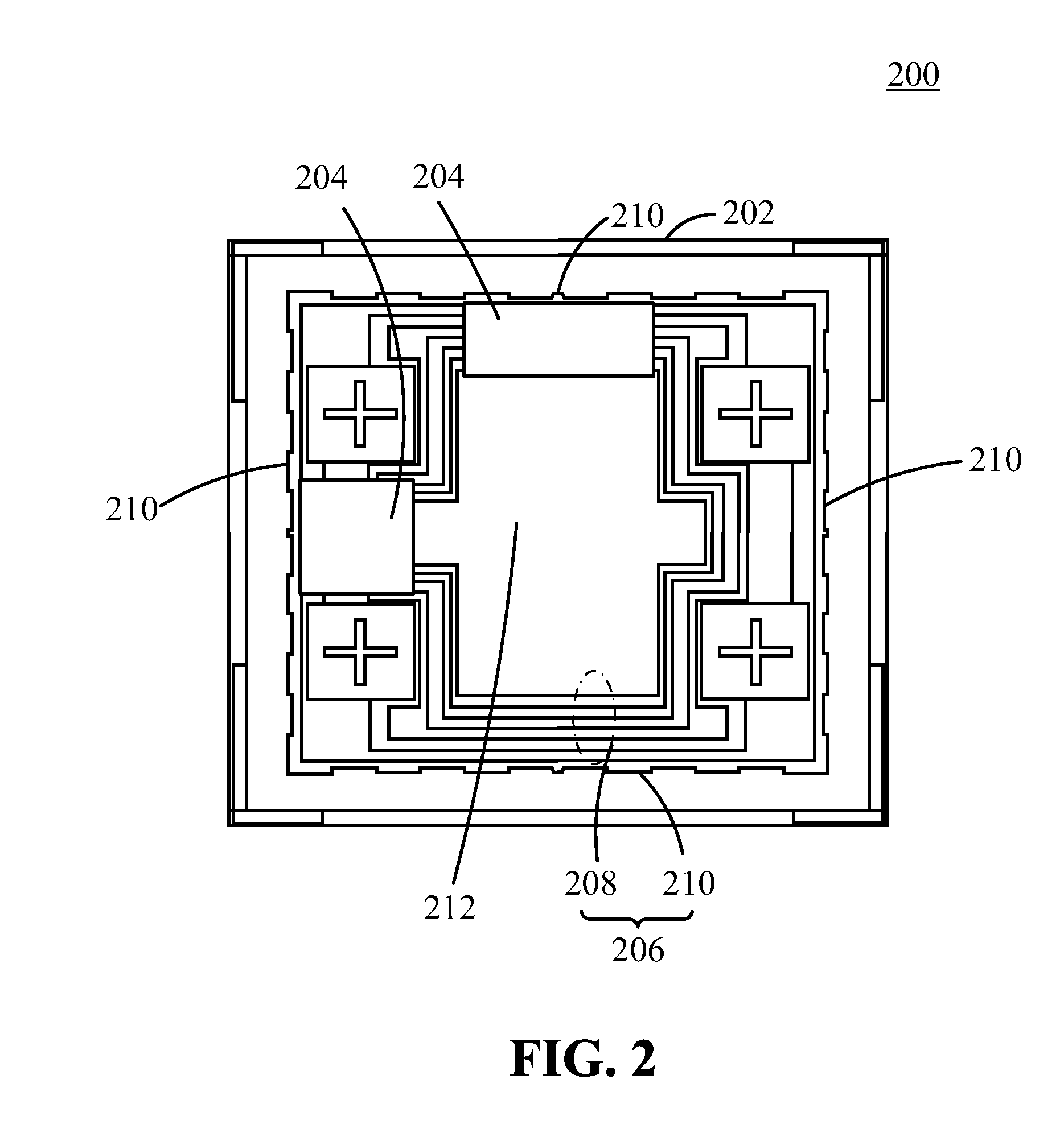
[0018]Please refer to FIG. 2. FIG. 2 illustrates a wiring structure of a liquid crystal display device 200 according to a first embodiment of the present invention. The wiring structure of the liquid crystal display device 200 comprises a substrate 202, a plurality of electrical elements 204, and a plurality of wirings 206. The substrate 202 is a glass substrate. The electrical elements 204 are disposed on the substrate 202 to generate a plurality of electrical signals for displaying an image. The electrical elements 204 comprise at least one gate driving circuit and at least one source driving circuit. In one embodiment, the gate driving circuit is a gate driving integrated circuit which is disposed on the substrate 202, and the source driving circuit is a source driving integrated circuit which is disposed on the substrate 202. In another embodiment, the gate driving circuit is manufactured on the substrate 202. The wirings 206 are coupled to the electrical elements 204 to transmi...


PUM

PropertyMeasurementUnit
distancesaaaaaaaaaa
resistanceaaaaaaaaaa
areasaaaaaaaaaa

Abstract

A wiring structure of a liquid crystal display device and a liquid crystal display device are disclosed. The wiring structure of the liquid crystal display device includes a substrate, plural electrical elements, and plural wirings. The electrical elements are disposed on the substrate to generate plural electrical signals. The wirings are coupled to the electrical elements to transmit the electrical signals. The wirings include inner wirings and an outermost peripheral wiring. The outermost peripheral wiring and the inner wirings have different wiring patterns. Each of the electrical elements is positioned at a side of the outermost peripheral wiring facing the center of the substrate. After the liquid crystal display device is cut and polished, by distinguishing the wiring patterns of both the outermost peripheral wiring and the inner wirings, the existence of the outermost peripheral wiring shows that the outermost peripheral wiring is not polished and removed.

Description

CROSS REFERENCE TO RELATED APPLICATION[0001]This application is a continuation-in-part of U.S. patent application Ser. No. 12 / 496,445, filed on Jul. 1, 2009, which is incorporated herein by reference in its entirety, and which itself claims priority under 35 U.S.C.§119(a) on Patent Application No. 098204804 filed in Taiwan, R.O.C. on Mar. 26, 2009, which is incorporated herein by reference in its entirety.TECHNICAL FIELD OF THE INVENTION[0002]The present invention relates to a wiring structure, and more particularly to a wiring structure of a liquid crystal display device which can easily be distinguished.BACKGROUND OF THE INVENTION[0003]A conventional wiring structure around the edges of a liquid crystal display device is a straight-line pattern. However, the development of the liquid crystal display device is progressing toward the widescreen types, therefore the edge areas for wirings are narrower than before. In addition, according to design with increased substrate utilization ...

Claims


Application Information

Patent Timeline
Patent Type & Authority Patents(United States)
IPC IPC(8): G02F1/1343G02F1/1345
CPCG02F1/1345G02F1/136286
Inventor LIN, YEN-FENHSU, HAN-TUNG
Owner CHUNGHWA PICTURE TUBES LTD
Learn More