Storage region allocation system, storage region allocation method, and control apparatus

a storage region and allocation method technology, applied in the field of memory control, can solve the problem that the desired data cannot be accessed, and achieve the effect of sped up accesses from a plurality of circuits that simultaneously occur, efficient omission, and speed up accesses

Inactive Publication Date: 2012-07-17
NEC CORP
View PDF17 Cites 2 Cited by
  • Summary
  • Abstract
  • Description
  • Claims
  • Application Information

AI Technical Summary

Benefits of technology

[0058]According to the present invention, accesses from a plurality of circuits that simultaneously occur can be sped up. The reason for the speeding up is that, in the present invention, the calculation means determines allocation of the external memory so that the number of necessary cycles is minimized, and further the access order determination means determines the access order so that transfer of high-order address is minimized.
[0059]In the SDRAM, for example, by optimizing allocation of memory spaces to be used by the respective circuits, the ACTIVE command and the PRECHARGE command can be efficiently omitted. The accesses can be thereby sped up.
[0060]Further, according to the present invention, the calculation means performs allocation with addresses put close to one another so that high-order addresses may be shared as much as possible. A usage rate of the external memory can be thereby increased.

Problems solved by technology

This is because several types of data occupy all the memory spaces, and unless the access is made this manner or unless the ACTIVE command is used, desired data cannot be accessed.

Method used


Image

  • Storage region allocation system, storage region allocation method, and control apparatus
  • Storage region allocation system, storage region allocation method, and control apparatus
  • Storage region allocation system, storage region allocation method, and control apparatus

Examples


example

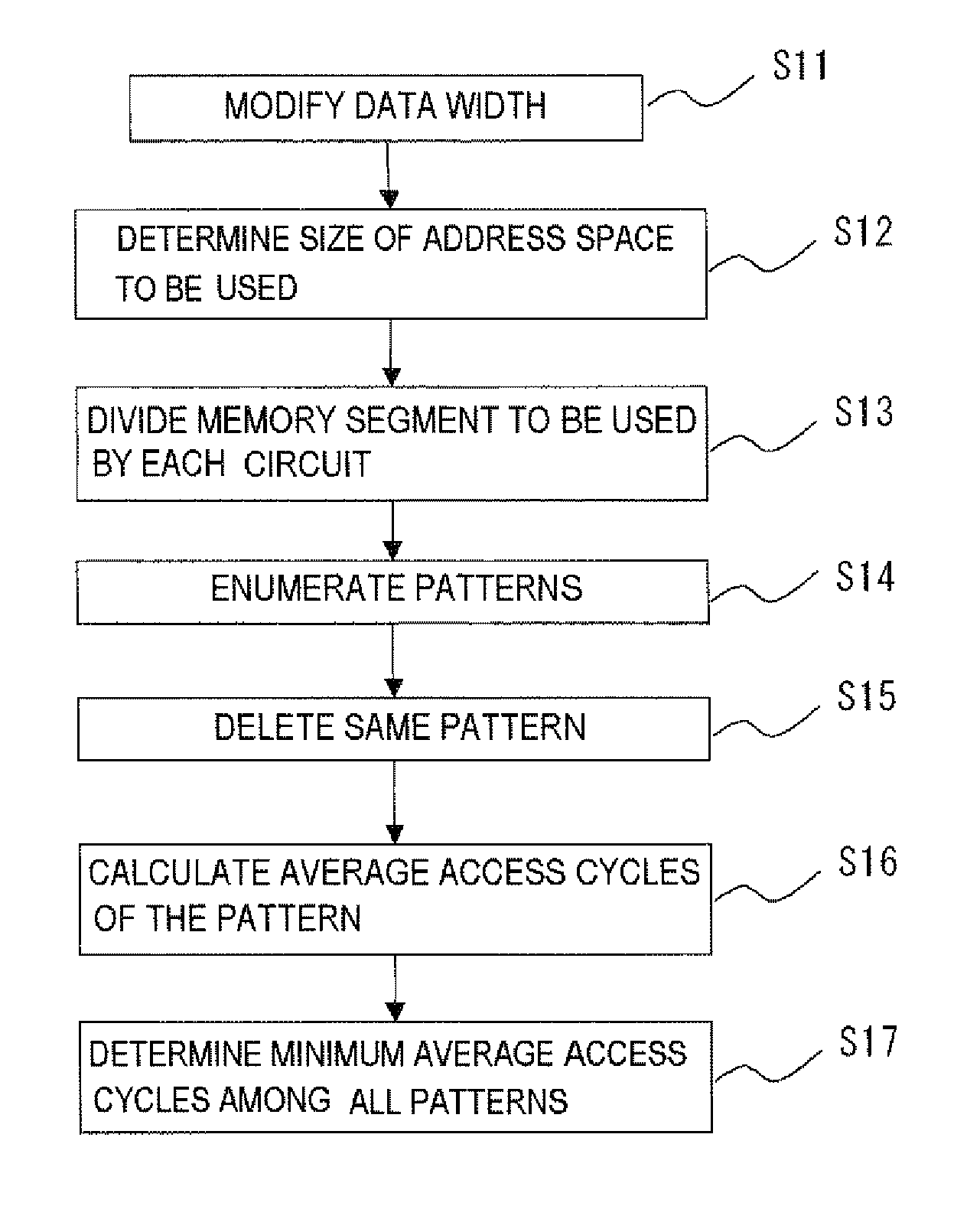
[0157]Referring to FIG. 16, a case where the respective means in the exemplary embodiment of the present invention are all implemented by circuits is shown. In the present example, the input means 502 are implemented as terminals of the calculation circuit 503. In other words, information on an address width of 10 bits of the circuit 1, a data width of 32 bits of the circuit 1, a high-order address width of 13 bits of the SDRAM, a low-order address width of 10 bits of the SDRAM, a data width of 64 bits of the SDRAM, and a data width to be influenced by the one-bit write enable and the like is directly input to the calculation circuit 503 as input signals. The external memory 505 is constituted from an SDRAM module.

[0158]Examples of numerical values of the address widths and the data widths and the like, shown in FIG. 16, are used simply as examples, and detailed examples of calculation will be omitted. An operation of the present example will be described below.

[0159]The calculation...


PUM


Abstract

There are provided a memory space allocation method and a memory space allocation device that aim at higher-speed accesses when a memory is shared by a plurality of circuits. In this memory, one data is accessed by issuing addresses a plurality of times. Memory allocation is performed so that high-order addresses of memory spaces of an external memory 505 may be maximally shared by a plurality of circuits 501. When the high-order addresses are common, a memory control circuit does not transfer the high-order addresses, thereby reducing the number of transfers of the high-order addresses. Therefore, the higher-speed access is achieved.

Description

TECHNICAL FIELD[0001]The present invention relates to memory control. More specifically, the invention relates to a memory region allocation system, a memory region allocation method, a control apparatus, and a computer program, for sharing one memory by a plurality of circuits, for use.BACKGROUND ART[0002]An increasing number of LSIs in recent years, such as those in multimedia systems and operating systems, need much memory (large-capacity memory) for processing. However, the capacity of the memory capable of being mounted on-chip on an LSI is often smaller than a required memory capacity. In such a case, a dedicated memory LSI is connected to the outside of the LSI for performing a desired process. In such a configuration, accesses to the external memory LSI are sometimes made from a plurality of circuits. In a memory control circuit, for example, arbitration control of accesses from a plurality of circuits is performed. Further, in recent years, a clock synchronous type dynamic ...

Claims


Application Information

Patent Timeline
Patent Type & Authority Patents(United States)
IPC IPC(8): G06F12/00G06F12/02
CPCG06F12/02G06F12/0215G06F13/1631G06F12/00G06F12/06
Inventor HOSOKAWA, KOUHEI
Owner NEC CORP
Why Eureka
Try Eureka