Deep submicron and nano CMOS single photon photodetector pixel with event based circuits for readout data-rate reduction communication system

a communication system and submicron and nano-cmos technology, applied in the field of sensor arrays, can solve the problems of large arrays, high operating voltage, easy damage, etc., and achieve the effect of reducing the size of the array to 3232 pixels, and reducing the size of the array

Active Publication Date: 2012-09-04
THE JOHN HOPKINS UNIV SCHOOL OF MEDICINE
View PDF9 Cites 63 Cited by
  • Summary
  • Abstract
  • Description
  • Claims
  • Application Information

AI Technical Summary

Problems solved by technology

Unfortunately, PMTs are bulky, easily damaged, expensive, susceptible to magnetic fields, and require high voltages for operation.
The resulting arrays were limited in size to 32×32 pixels, and required significant post-processing to connect readout circuitry.
Unfortunately, commercially available SPADs manufactured using high voltage CMOS processes suffer from reliability issues that limit the technology to feature sizes that are not competitive with low-voltage deep submicron and nano CMOS.
This limits the ultimate density and usability of SPAD arrays manufactured using high voltage CMOS processes, to applications that do not require high quality or dense detector arrays.
Fabrication steps that work to guarantee high breakdown voltages and eliminate latch-up often introduce leakage problems at crucial device interfaces.
The high dark count is likely the result of using STI material to form a guard ring, which creates a poor material interface at a crucial location inside the device and fails to buffer the bottom corners of the multiplication region from undesirable edge effects.

Method used


Image

  • Deep submicron and nano CMOS single photon photodetector pixel with event based circuits for readout data-rate reduction communication system
  • Deep submicron and nano CMOS single photon photodetector pixel with event based circuits for readout data-rate reduction communication system
  • Deep submicron and nano CMOS single photon photodetector pixel with event based circuits for readout data-rate reduction communication system

Examples


Embodiment Construction

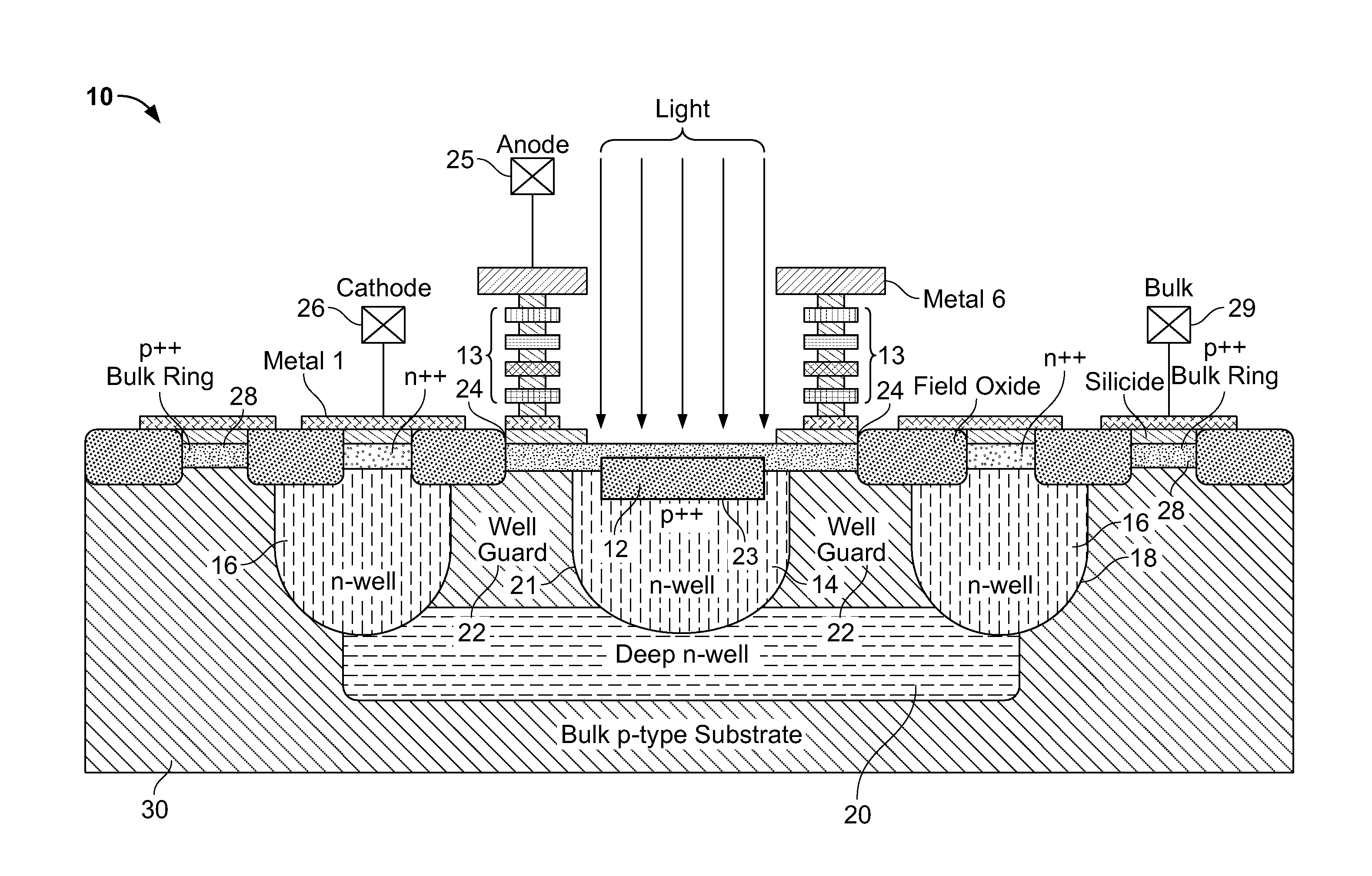
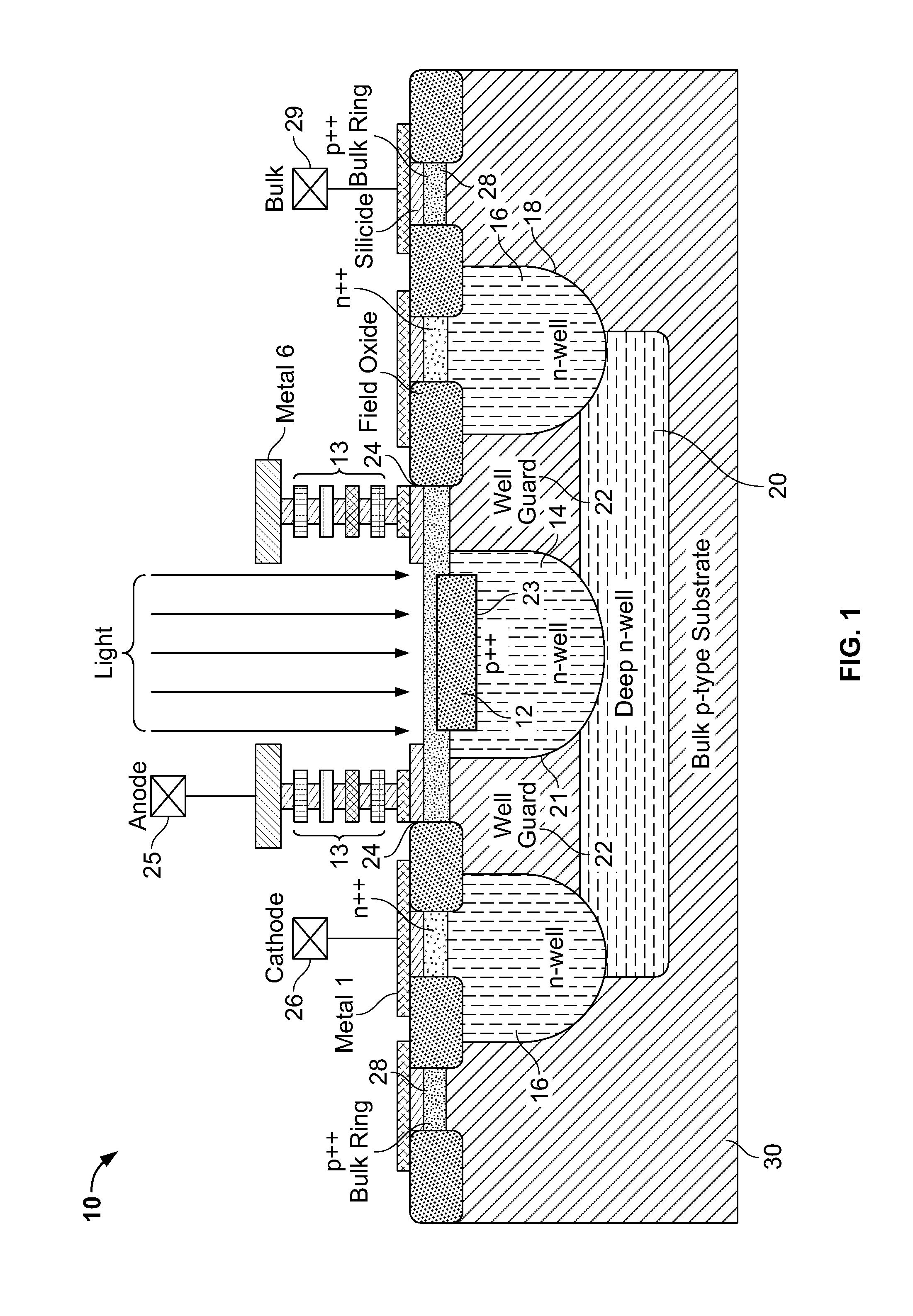
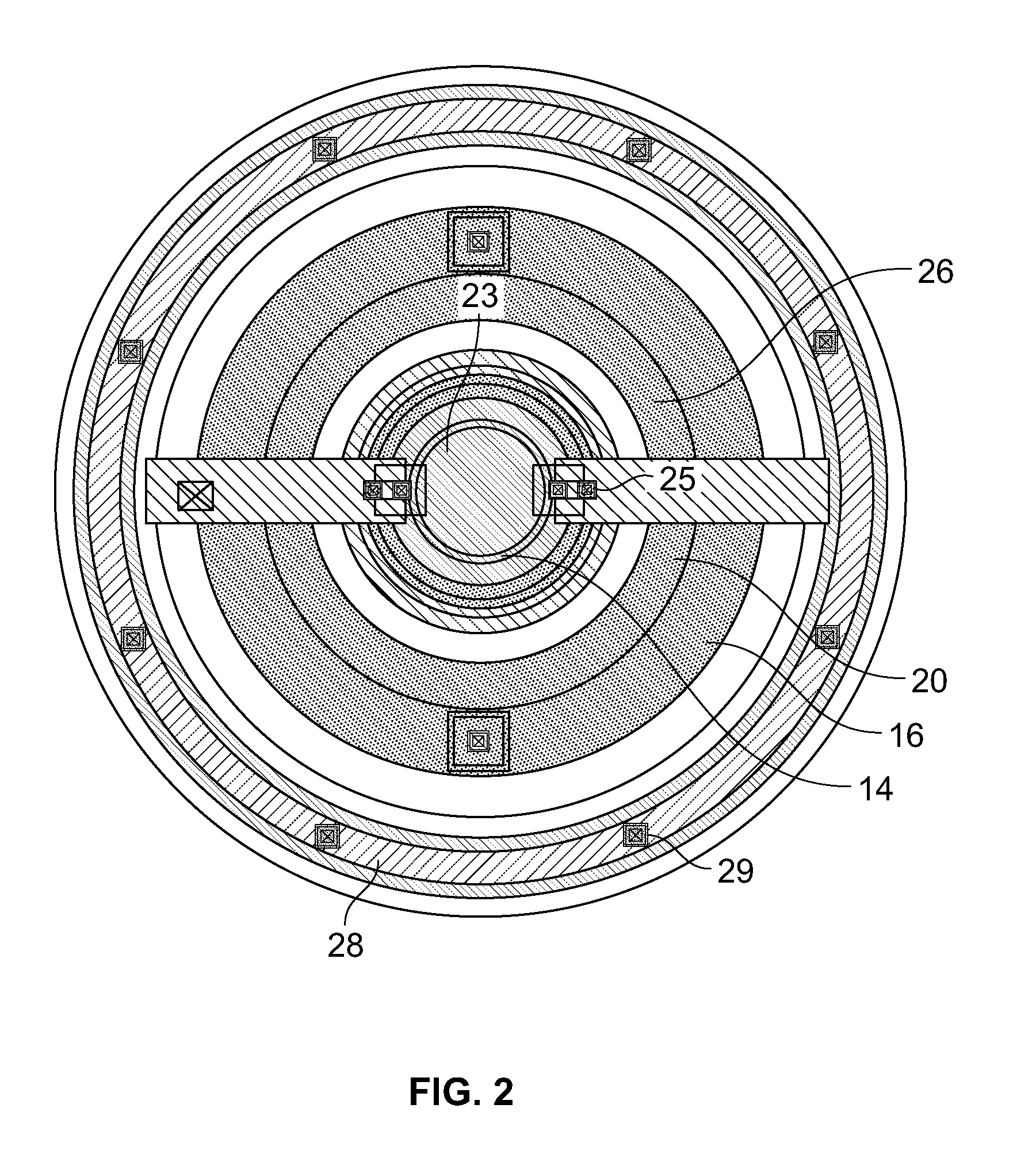
[0037]Disclosed herein is a design for building avalanche photodiodes that are free of edge effects at both the lateral and bottom sides of the junctions involved. Further described herein are pixel circuits incorporating such avalanche photodiodes which exhibit minimal dark counts that are manufactured using a low voltage, deep-submicron and nano CMOS foundry process. When the avalanche photodiodes are incorporated into an array of sensor array pixels, each of the pixels produces a digital output which can be used in an array readout such that the pixel size does not increase in size with the number of pixels in the array—signifying a big breakthrough in the design of large monolithic arrays of low-light level sensors. To achieve large arrays with high resolution (10000×10000 pixels), a small size pixel detector and a large transistor count in the pixel is needed to implement state holding and tagging elements such as counters and other processing circuits. This is made possible by...


PUM

PropertyMeasurementUnit
diameteraaaaaaaaaa
breakdown voltageaaaaaaaaaa

Abstract

An avalanche photodiode is disclosed. The avalanche photodiode includes a substrate of a first conductivity type. A first well of a second conductivity type is formed within the substrate. A second well of the second conductivity type is formed substantially overlying and extending into the first well. A heavily doped region of the first conductivity type is formed substantially overlying and extending into the first well, the junction between the heavily doped region and the second well forming an avalanche multiplication region. A guard ring is formed from a first conductivity material positioned substantially about the periphery of the multiplication region at least partially underlying the heavily doped region. An outer well ring of the second conductivity type is formed about the perimeter of the deep well and the guard ring.

Description

CROSS-REFERENCE TO RELATED APPLICATIONS[0001]This application is a U.S. National Phase Application of PCT International Application No. PCT / US2008 / 057205, filed Mar. 17, 2008, now published as WO 2008 / 113067, which claims the benefit of U.S. provisional patent application No. 60 / 918,268 filed Mar. 15, 2007, the disclosure of which is incorporated herein by reference in its entirety.FIELD OF THE INVENTION[0002]The present invention relates generally to sensor arrays, and more particularly to a deep submicron and nano CMOS-fabricated avalanche photodiode design and resulting pixel for incorporation into one and two dimensional sensor arrays.BACKGROUND OF THE INVENTION[0003]Optical sensors for extreme low-level light conditions can convert single photons into a measurable electrical signal. Single-photon detectors, as these sensors are called, can be employed in vision systems with 3D imaging and range capability, for sensing at night or in caves, for low data rate intra- and inter-pla...

Claims


Application Information

Patent Timeline
Patent Type & Authority Patents(United States)
IPC IPC(8): G01J1/42
CPCH01L27/14603H01L31/107
Inventor ANDREOU, ANDREAS G.MARWICK, MIRIAM ADLERSTEINPOULIQUEN, PHILIPPE O.
Owner THE JOHN HOPKINS UNIV SCHOOL OF MEDICINE
Why Eureka
Try Eureka