Group iii-nitride growth on silicon or silicon germanium substrates and method and devices therefor

a technology of group iii-nitride and silicon germanium, which is applied in the direction of semiconductor devices, lasers, semiconductor lasers, etc., can solve the problems of high cost of fabrication, difficult epitaxy of high-quality group iii-nitride films on silicon (si) rather than sic, and inability to meet the requirements of large-scale production

Inactive Publication Date: 2008-06-05
NAVY U S A AS REPRESENTED BY THE SEC OF THE THE
View PDF12 Cites 234 Cited by
  • Summary
  • Abstract
  • Description
  • Claims
  • Application Information

AI Technical Summary

Benefits of technology

[0009]The foregoing and other features and advantages of the present invention will be apparent from the following, more particular description of a preferred embodiment of the invention, as illustrated in the accompanying drawings.

Problems solved by technology

SiC and sapphire substrates represent a significant portion of the overall cost to fabricate a LED.
Unfortunately, SiC is not available in large diameters and is exceedingly expensive particularly for high-purity, insulating SiC, which is the preferred substrate for a group III-nitride high electron mobility transistors (HEMTs).
Epitaxy of high-quality group III-nitride films on silicon (Si), rather than SiC, is difficult due to the large lattice and thermal expansion coefficient mismatch between the group III-nitride film and the Si substrate.
For example, volume production of GaN LEDs deposited on Si substrates is generally plagued with high defect and crack density in group III-nitride films because of the large lattice and thermal expansion mismatch with the Si substrate.
However, the addition of such a SL or buffer layer, while allowing for a crack free and reduced defect GaN layer, causes distorted reflectance because of the buffer layers presence and thus is not particularly well suited for optoelectric applications such as an LED.

Method used


Image

  • Group iii-nitride growth on silicon or silicon germanium substrates and method and devices therefor
  • Group iii-nitride growth on silicon or silicon germanium substrates and method and devices therefor
  • Group iii-nitride growth on silicon or silicon germanium substrates and method and devices therefor

Examples


Embodiment Construction

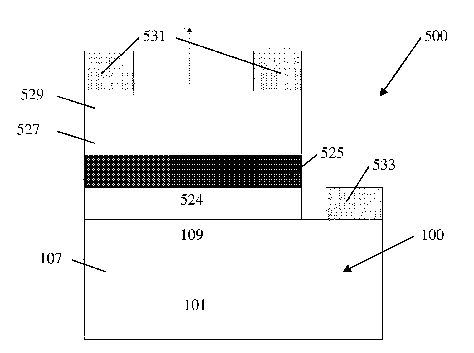
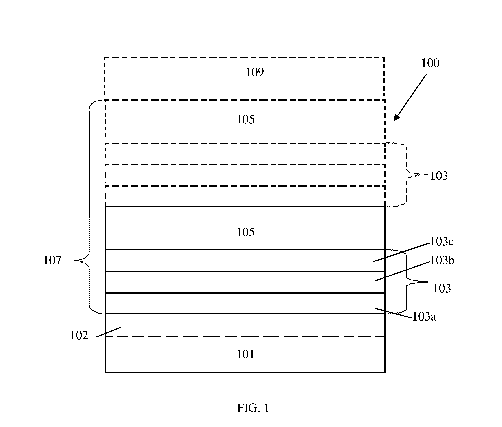
[0025]Preferred embodiments of the present invention are now described with reference to the Figures, in which like reference numerals are generally used to indicate identical or functionally similar elements. Also in the Figures, the left most digit of each reference numeral generally corresponds to the Figure in which the reference numeral appears. While specific details of the preferred embodiments are discussed, it should be understood that this is done for illustrative purposes only. A person skilled in the relevant art will recognize that other configurations and arrangements can be used without departing from the spirit and scope of the invention. It will also be apparent to a person skilled in the relevant art that this invention can also be employed in other applications.

[0026]The present invention includes a structure in which a SiC or sapphire substrate has been substituted with a silicon (Si) substrate or a Si and germanium (Ge) alloy substrate. Specifically, the present...


PUM

PropertyMeasurementUnit
reflectanceaaaaaaaaaa
sizeaaaaaaaaaa

Abstract

A structure including a Si1-xGex substrate and a distributed Bragg reflector layer disposed directly onto the substrate. The distributed Bragg reflector layer includes a repeating pattern that includes at least one aluminum nitride layer and a second layer having the general formula AlyGa1-yN. Another aspect of the present invention is various devices including this structure. Another aspect of the present invention is directed to a method of forming such a structure comprising providing a Si1-xGex substrate and depositing a distributed Bragg reflector layer directly onto the substrate. Another aspect of the present invention is directed to a photodetector or photovoltaic cell device, including a Si1-xGex substrate device, a group III-nitride device and contacts to provide a conductive path for a current generated across at least one of the Si1-xGex substrate device and the group III-nitride device upon incident light.

Description

FIELD OF THE INVENTION[0001]The present invention is generally directed to a group III-nitride structure grown on silicon or silicon germanium alloy substrates, devices having this structure and the manufacture thereof.BACKGROUND OF THE INVENTION[0002]The group III-nitride family of materials can be fabricated into optoelectronic devices that emit or absorb light in the ultraviolet (UV) and the entire visual spectrum. There is a large commercial market for, for example, GaN-based light emitting diodes (LEDs) and edge-emitting lasers that emit light in the UV, blue and green wavelength ranges. In the future it is expected that a number of additional devices, including vertical cavity surface emitting lasers (VCSELs) and resonant cavity light emitting diodes (RCLEDs) will be commercialized based on the group III-nitride material.[0003]Deposition of group III-nitride films is typically conducted on expensive silicon carbide (SiC) or sapphire, i.e., aluminum oxide, substrates. SiC and s...

Claims


Application Information

Patent Timeline
Patent Type & Authority Applications(United States)
IPC IPC(8): H01L31/0336H01L31/0232H01L31/18
CPCH01L31/078Y02E10/544H01L31/184H01L31/1812
Inventor MASTRO, MICHAEL A.EDDY, CHARLES R.AKBAR, SHAHZAD
Owner NAVY U S A AS REPRESENTED BY THE SEC OF THE THE
Why Eureka
Try Eureka