Surface mount semiconductor device

a semiconductor device and surface mount technology, applied in semiconductor devices, semiconductor/solid-state device details, electrical equipment, etc., can solve the problems of requiring precision alignment, several extra process steps, and limited devices

Active Publication Date: 2012-10-09
NXP USA INC
View PDF7 Cites 5 Cited by
  • Summary
  • Abstract
  • Description
  • Claims
  • Application Information

AI Technical Summary

Problems solved by technology

This technique is limited to devices where the exposed electrical contacts of the package are disposed around the periphery of the semiconductor die.
However, the process requires deposition and patterning of several layers, requiring precision aligning and several extra process steps, especially for complex redistribution.

Method used


Image

  • Surface mount semiconductor device
  • Surface mount semiconductor device
  • Surface mount semiconductor device

Examples


Embodiment Construction

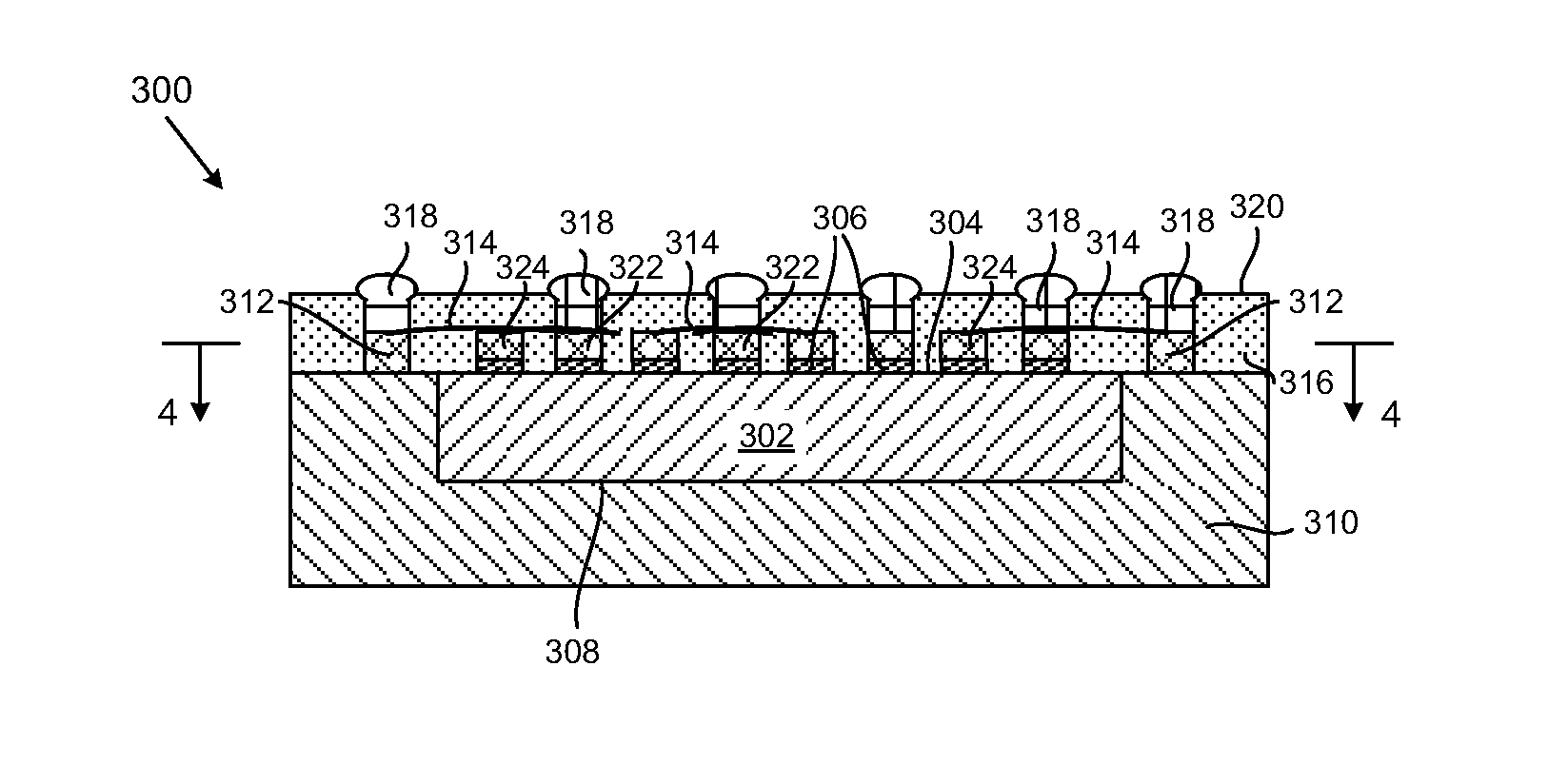
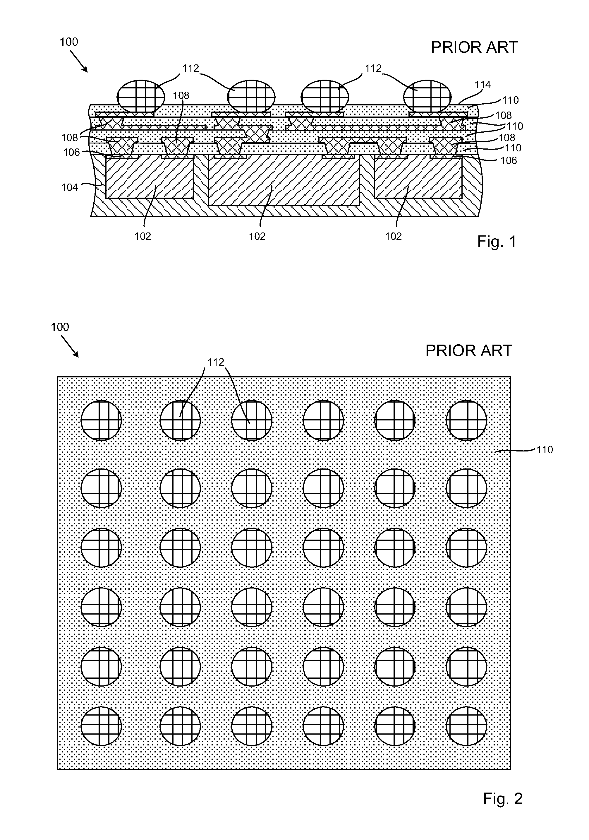
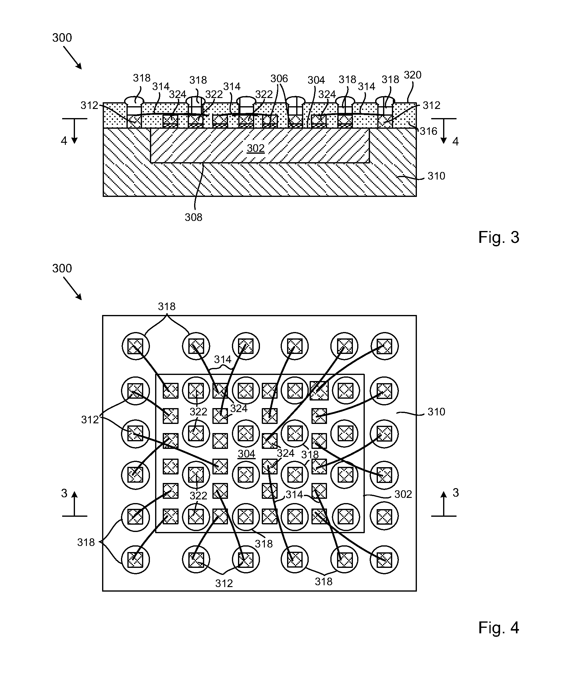
[0016]FIGS. 1 and 2 show a known redistributed chip package (‘RCP’) semiconductor device 100. The semiconductor device 100 includes one or more (in this case three) singulated semiconductor dies 102 embedded in a molding compound 104 with electrical contact pads such as 106 at a surface of the molding compound. A plurality of electrically conductive layers and vias 108, separated by insulating layers 110, are formed on the surface of the molding compound and provide interconnections between the semiconductor dies 102 and with an array of solder balls 112 at an active face 114 of the device 100. Patterning of the electrically conductive layers and vias 108 enables the array or arrays of pads 106 on the semiconductor dies 102 to be redistributed geometrically, so that the array of solder balls 112 at the active face 114 of the device 100 may have a different geometry from the geometry of the pads 106 on the semiconductor dies 102.

[0017]During manufacture, the singulated semiconductor ...


PUM


Abstract

A surface mount semiconductor device has a semiconductor die encapsulated in a molding compound. Electrical contact elements of an intermediate set are disposed on the molding compound. A set of coated wires electrically connect bonding pads of the semiconductor die and the electrical contact elements of the intermediate set. A layer of insulating material covers the coated wires, the die and the electrical contact elements of the intermediate set. Electrically conductive elements are exposed at an external surface of the layer of insulating material and contact respective electrical contact elements of the intermediate set through the layer of insulating material.

Description

BACKGROUND OF THE INVENTION[0001]The present invention is directed to a surface mount semiconductor device and to a method of assembling a surface mount semiconductor device.[0002]Semiconductor device packaging fulfills basic functions such as providing electrical connections and protecting the die against mechanical and environmental stresses. Continued progress in reduction of the size of the semiconductor dies and increased functionality and complexity of the circuits integrated in the dies require size reduction of the packaging with the same or greater complexity of the electrical connections with external circuits.[0003]Semiconductor devices are commonly packaged for surface mounting by encapsulating one or more semiconductor dies with a mold compound. Electrical contacts for connection with external circuits are exposed in an active face of the package and are connected internally with electrical contact pads on the semiconductor die. Various techniques are available for conn...

Claims


Application Information

Patent Timeline
Patent Type & Authority Patents(United States)
IPC IPC(8): H01L23/48
CPCH01L23/3128H01L23/5389H01L24/96H01L21/561H01L21/568H01L24/05H01L23/49816H01L2224/0401H01L2224/24137H01L2924/01029H01L2924/01047H01L2924/01079H01L2924/01082H01L2924/01033H01L2924/01075H01L2924/014H01L2224/12105H01L2224/02319H01L2224/02381H01L2224/13023H01L2224/13024H01L2924/00014H01L2924/181H01L2924/00
Inventor LO, WAI YEWKHOO, LY HOONKOH, WEN SHI
Owner NXP USA INC
Why Eureka
Try Eureka