Field probe

a field probe and probe body technology, applied in the field of field probes, can solve the problems of difficult mechanically reliable connection and manufacturing difficulties, and achieve the effects of improving performance, flat frequency response, and less manufacturing cos

Active Publication Date: 2012-11-06
AMPLIFIER RES
View PDF3 Cites 2 Cited by
  • Summary
  • Abstract
  • Description
  • Claims
  • Application Information

AI Technical Summary

Benefits of technology

[0017]Each of the circuit boards has first and second opposite faces, and the thin film resistive elements are disposed on a first face of each circuit board with conductive pads for making electrical connections to the thin film resistive elements. In a preferred embodiment, each circuit board includes a first masking layer covering substantially the entire first face thereof, except at the locations of the conductive pads, for preventing solder from adhering to parts of the circuit boards other than said conductive pads. Substantially the entire second face of each circuit board is also covered by a second masking layer having a surface tension substantially the same as that of the first masking layer.
[0023]By virtue of the incorporation of each dipole and its feedline on a common circuit board, the probe can be manufactured less expensively, and can exhibit improved performance particularly by way of a comparatively flat frequency response, a broad frequency range, and low isotropic deviation. In addition, the fact that the circuit board arms are received in slots formed inside the RF-transparent housing makes it possible to indicate the positions and orientation of the dipoles by providing markings on the exterior of the RF-transparent housing.

Problems solved by technology

Problems encountered with conventional broadband field probes of the kind mentioned above include difficulties in measuring DC voltage across a detector diode situated at the mid-point of a short dipole, avoidance of metal objects near the sensors, and avoidance of conductors for coupling the sensors to the electronic circuitry.
The connections between the feed lines and the sensing elements give rise to manufacturing difficulties.
It is difficult to make mechanically reliable connections that do not impair the probe's frequency response.

Method used


Image

  • Field probe
  • Field probe
  • Field probe

Examples


Embodiment Construction

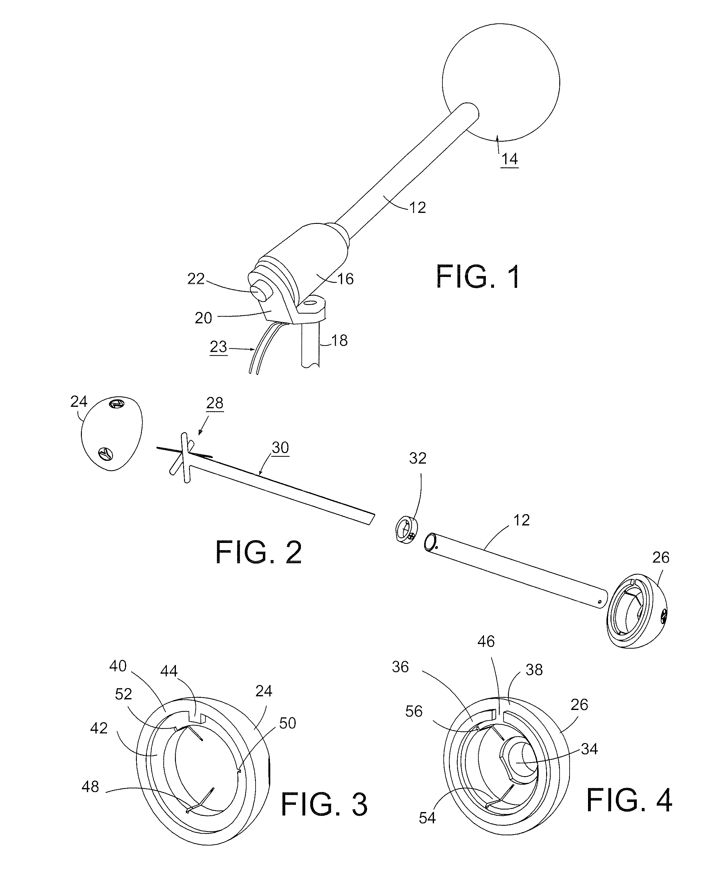
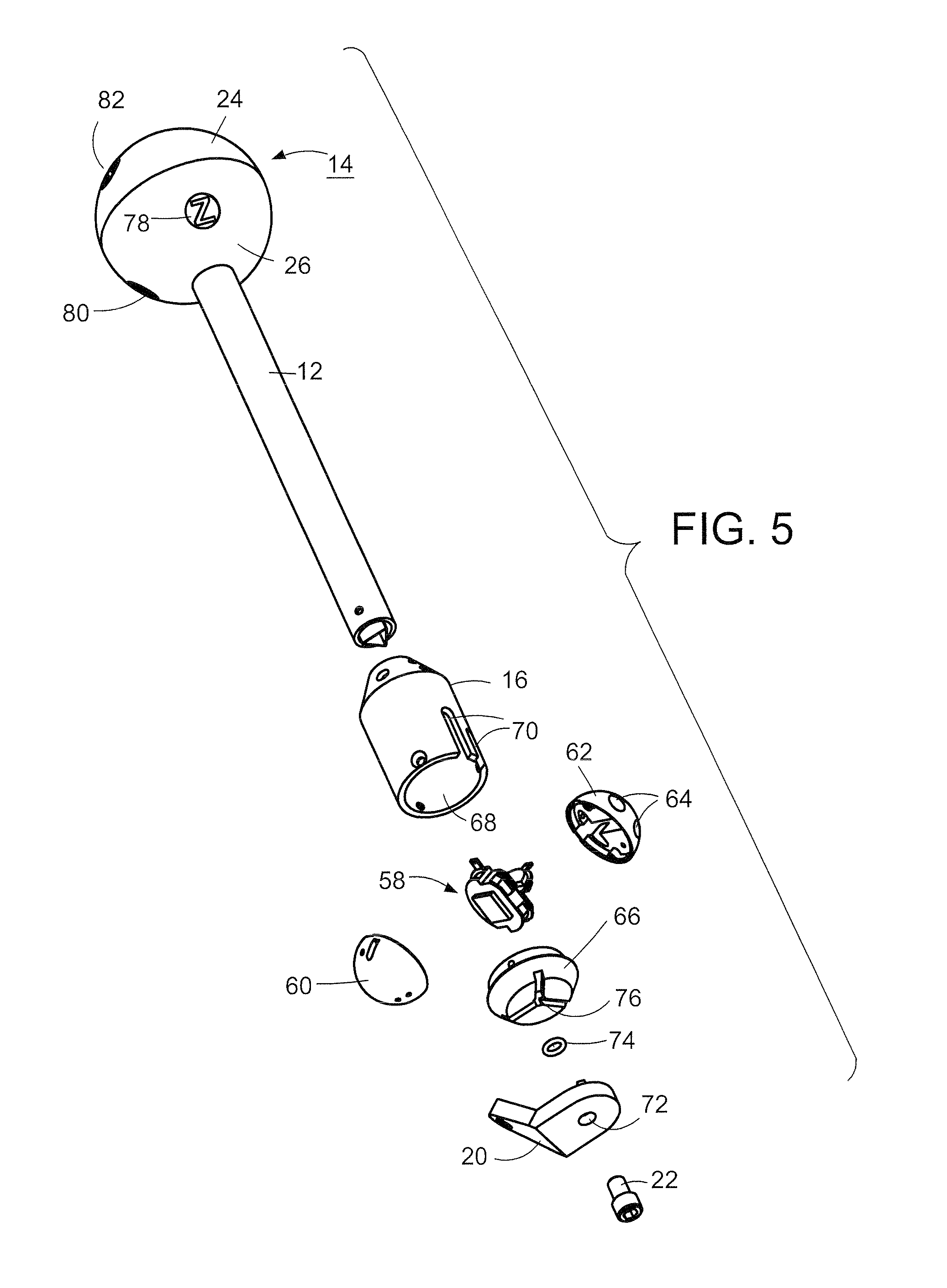
[0036]The field probe as shown in FIG. 1 comprises a tubular stalk 12 having a spherical, radio frequency-transparent housing 14 at one end and an electronic circuit housing 16 at the opposite end. The electronic circuit housing 16 is supported on a vertical post 18 by a bracket 20, which is configured so that the axis of the stalk is disposed at an angle relative to a horizontal plane corresponding to the angle between the diagonal of a cube and its base, i.e., approximately 35.3°. The electronic circuit housing 16 is secured to the bracket 20 by a screw 22, which can be loosened to allow rotation of the probe about the axis of the stalk. As will appear from the description to follow, the dipoles are disposed at 54.7° (90°-35.3°) relative to the stalk axis. Consequently any one of the dipoles can be brought to a vertical position by rotation of the probe about the stalk axis, and the three dipoles inside the RF-transparent housing 14 can be oriented in relation to mutually perpendi...


PUM


Abstract

In a stalk-type field probe, each of three resistive dipoles is formed with a resistive feedline on a common circuit board. Each circuit board comprises an elongated feedline section that extends through a cylindrical stalk, and a cross-arm that is disposed at a 54.7° angle relative to the elongation of the feedline section. The feedline sections are arranged to form an equilateral triangular prism, and the cross arms are arranged so that the dipole on each cross-arm is perpendicular to an imaginary plane to which the lines along which the elements of both of the other dipoles extend are parallel.

Description

FIELD OF THE INVENTION[0001]This invention relates to field probes for use in measuring electromagnetic fields in high frequency applications, and more particularly to an improved field probe for use in electric field measurements.BACKGROUND OF THE INVENTION[0002]Field probes are used in evaluating the performance of many different kinds of radio frequency equipment, and are also essential components of radiated immunity testing systems for use in ensuring that electrical and electronic and systems in products such as automobiles are not adversely affected by stray fields such as radio and television transmissions, radar pulses, cellular telephone signals, powerline fields, and the other kinds of electromagnetic fields.[0003]Several different kinds of field probes are used in the above-mentioned applications. These include cube probes, sphere probes, and so-called “stalk probes.” A typical cube probe includes three mutually perpendicular sensing elements extending from three faces o...

Claims


Application Information

Patent Timeline
Patent Type & Authority Patents(United States)
IPC IPC(8): H01Q21/00
CPCH01Q21/26H01Q1/42H01Q1/248G01R29/0878G01R1/06G01R29/08
Inventor GALLUPPI, JASON
Owner AMPLIFIER RES
Why Eureka
Try Eureka