Photosensitive device and method of manufacturing a photosensitive device using nanowire diodes

a nanowire diode and photosensitive technology, applied in the direction of radiation controlled devices, optical radiation measurement, instruments, etc., can solve the problem of insufficient photosensitivity of conventionally manufactured devices, and achieve the effect of low effort and low cos

Active Publication Date: 2012-12-11
NXP BV
View PDF12 Cites 41 Cited by
  • Summary
  • Abstract
  • Description
  • Claims
  • Application Information

AI Technical Summary

Benefits of technology

[0021]According to an exemplary embodiment of the invention, a photosensitive device may be characterized by the vertical alignment of the nanowire diodes each being sensitive to a specific wavelength portion of electromagnetic radiation, wherein the vertical alignment architecture may simplify the manufacture procedure, may make the device more sensitive to different spectral portions, and may contribute to the miniaturization of the device.
[0046]Alternatively, the plurality of vertically aligned nanowire diodes may also be formed by a growth procedure to extend essentially vertically relative to a surface of the substrate. In order to define the diameter of the nanowires during the growing procedure, it is possible to deposit an array of spots of catalysts material on a substrate for catalyzing the growth of the nanowires. For instance, for growing carbon nanotubes, iron or nickel spots may be used as such a catalyst. By dimensioning the spots in accordance with the desired diameters of the nanowires to be grown on the spots, any structure of nanowire diodes having different diameters may be manufactured easily.

Problems solved by technology

However, a sufficient photosensitivity of the conventionally manufactured devices cannot be guaranteed.

Method used


Image

  • Photosensitive device and method of manufacturing a photosensitive device using nanowire diodes
  • Photosensitive device and method of manufacturing a photosensitive device using nanowire diodes
  • Photosensitive device and method of manufacturing a photosensitive device using nanowire diodes

Examples


Embodiment Construction

[0068]The illustration in the drawing is schematical. In different drawings, similar or identical elements are provided with the same reference signs.

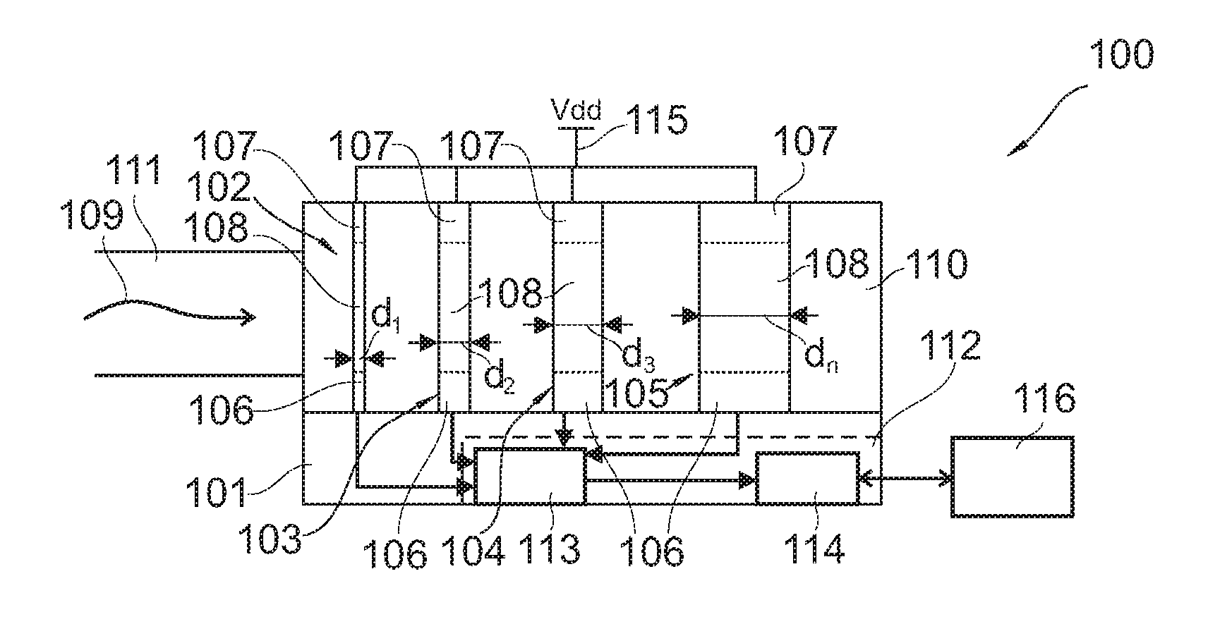
[0069]In the following, referring to FIG. 1, a photosensitive device 100 according to an exemplary embodiment of the invention will be explained.

[0070]The photosensitive device 100 comprises a silicon substrate 101. A plurality of vertically aligned nanowire diodes 102 to 105 is formed on the silicon substrate 101. As can be taken from FIG. 1, the different nanowire diodes 102 to 105 have different diameters d1 to d4 to thereby be sensitive to different spatial portions of electromagnetic radiation, particularly light. The nanowire diodes 102 to 105 are provided parallel to each other and comprise a first end portion 106 being p-doped and comprise a second end portion 107 being n-doped. The substrate 101 in this case is also p-doped.

[0071]Between the n-doped portion 107 and the p-doped portion 106, an essentially non-doped or intrinsic...


PUM

PropertyMeasurementUnit
diameteraaaaaaaaaa
diameteraaaaaaaaaa
lengthaaaaaaaaaa

Abstract

A photosensitive device (100), the photosensitive device (100) comprising a substrate (101) and a plurality of vertically aligned nanowire diodes (102 to 105) provided on and / or in the substrate (101).

Description

FIELD OF THE INVENTION[0001]The invention relates to a photosensitive device.[0002]Moreover, the invention relates to a method of manufacturing a photosensitive device.[0003]Beyond this, the invention relates to methods of using a photosensitive device.BACKGROUND OF THE INVENTION[0004]Opto-electronic components for silicon integrated circuits are considered for use to distinguish between different wavelengths of incident light. Such components can be used for analyzing the spectrum of various light sources. Conventional planar technology is normally used to manufacture structures showing this effect.[0005]JP 60091668 discloses a planar light-receiving integrated element to give an IC itself characteristics as an optical filter, and to reduce the areas of mounting of elements. This shall be achieved by forming a plurality of photodiodes having different sensitivity to the wavelengths of beams on the same substrate, signal-conditioning output currents from each diode and using several...

Claims


Application Information

Patent Timeline
Patent Type & Authority Patents(United States)
IPC IPC(8): G01J1/42
CPCH01L27/1446H01L31/0352
Inventor AGARWAL, PRABHAT
Owner NXP BV
Why Eureka
Try Eureka