Infrared sensor structure and method

a sensor and infrared technology, applied in the field of infrared sensor structure and method, can solve the problems of large, expensive packages, and large equipment setup requirements of above described prior art ir sensors, and achieve the effect of small and less expensiv

Active Publication Date: 2010-08-26
TEXAS INSTR INC
View PDF25 Cites 29 Cited by
  • Summary
  • Abstract
  • Description
  • Claims
  • Application Information

AI Technical Summary

Benefits of technology

[0021]It is an object of the invention to provide an IR radiation sensor which is substantially smaller and less expensive than the IR radiation sensors of the prior art.

Problems solved by technology

The prior art calibration procedure is very sensitive to the equipment set-up and to the variances and accuracy of the various components of the equipment set-up.
The above described prior art IR sensors require large, expensive packages.
Furthermore, the “floating” portion of dielectric membrane over cavity 4 in Prior Art FIG. 1 is quite fragile.
This creates a large opening span that is difficult to protect.

Method used


Image

  • Infrared sensor structure and method
  • Infrared sensor structure and method
  • Infrared sensor structure and method

Examples


Embodiment Construction

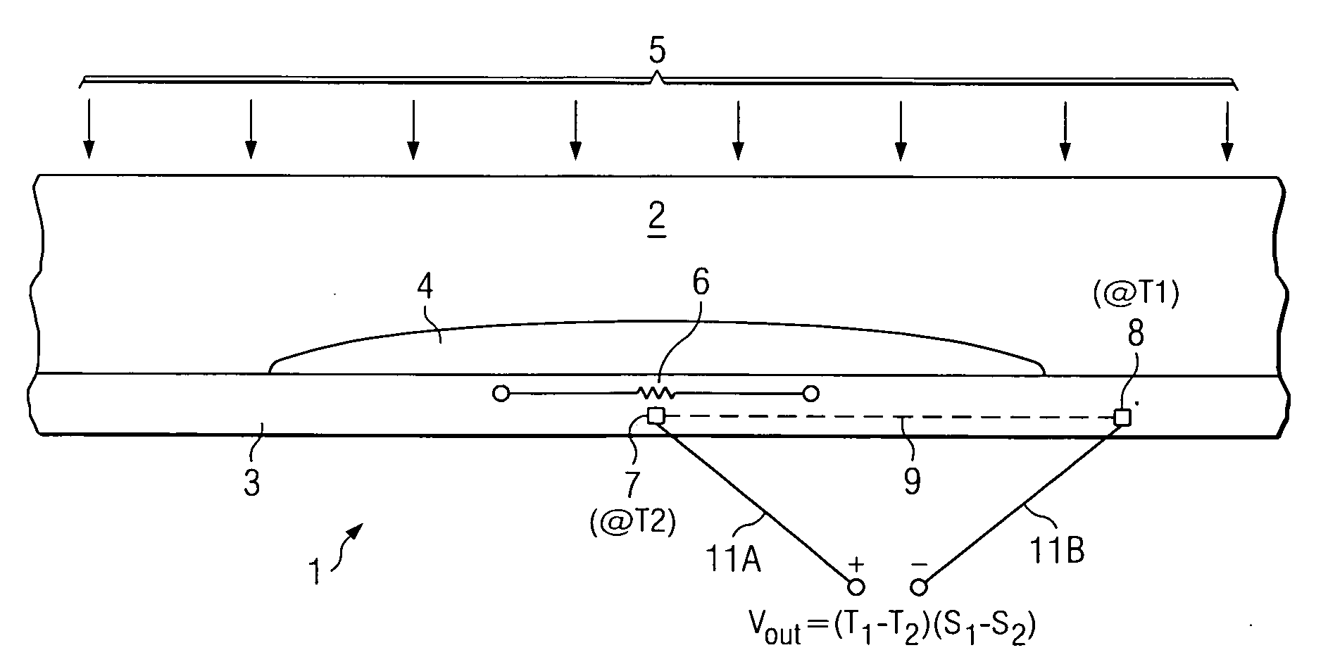
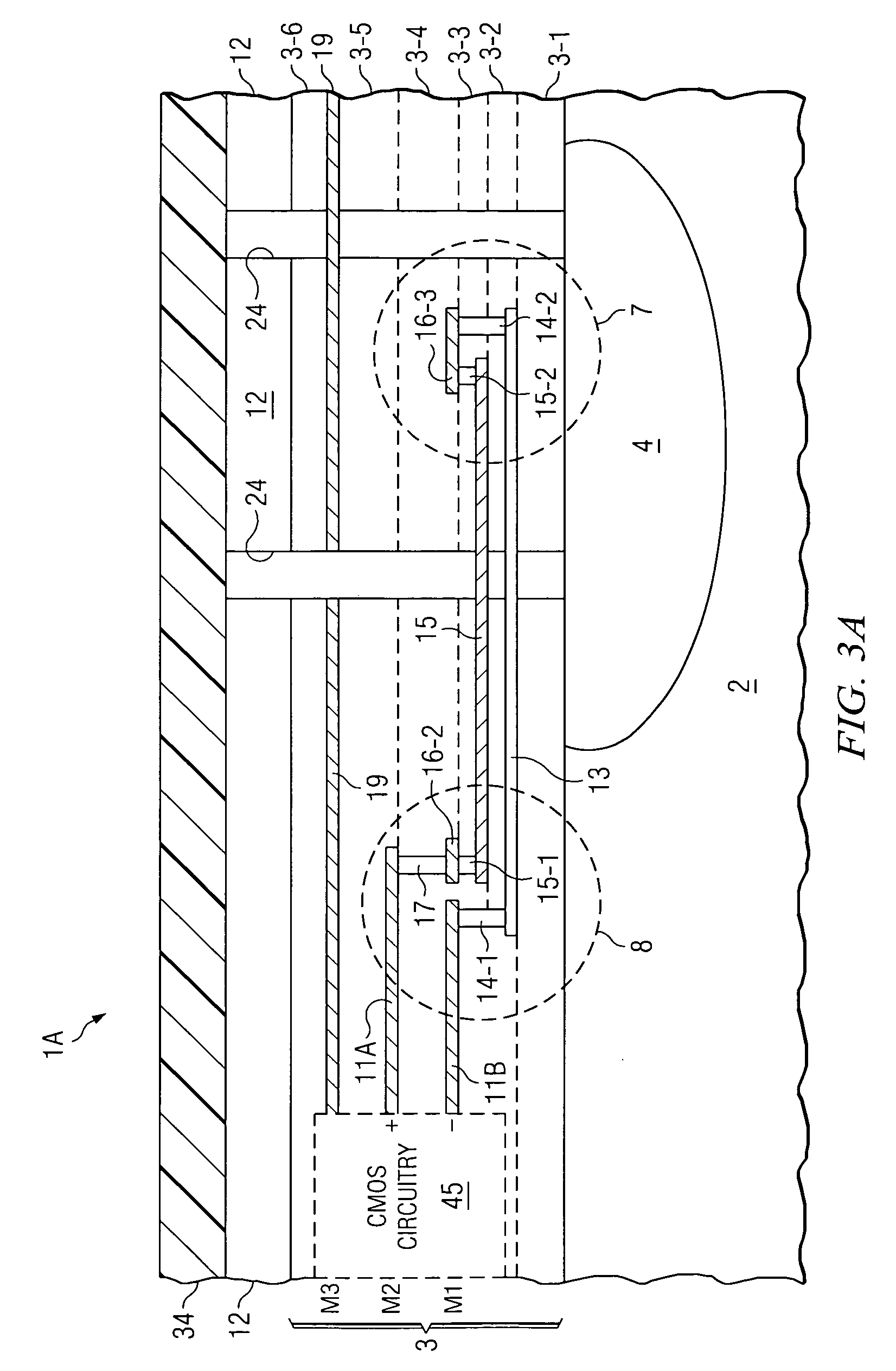
[0050]FIG. 2 shows a schematic representation of a IR sensor chip 1 of the present invention, with the sensor chip 1 inverted relative to the orientation shown in FIG. 1. In FIG. 2, IR detector chip 1 includes silicon substrate 2 in which cavity 4 is formed. A conventional CMOS-processing-compatible SiO2 dielectric stack 3 is formed on the lower surface of silicon substrate 2. The upward-oriented back surface of silicon substrate 2 receives IR radiation 5 and passes it through to SiO2 stack 3 while filtering out any ambient visible light. SiO2 stack 3 may contain various aluminum traces, polysilicon traces, and various other traces and metal contacts that are available in some conventional CMOS wafer fabrication processes. A first thermopile junction 7 is formed by dissimilar materials within dielectric stack 3 adjacent to cavity 4, and is thermally insulated, by cavity 4, from silicon substrate 2. A second thermopile junction 8 is formed by dissimilar materials within dielectric st...


PUM


Abstract

A radiation sensor (27) includes a radiation sensor chip (1) including first (7) and second (8) thermopile junctions connected to form a thermopile (7,8). The first thermopile junction is disposed in a floating portion of a dielectric membrane (3) thermally insulated from a silicon substrate (2) of the chip, and the second thermopile junction is disposed in the dielectric membrane directly adjacent to the substrate. Bump conductors (28) are bonded to corresponding bonding pads (28A) coupled to the thermopile (7,8) to physically and electrically connect the chip to conductors on a printed circuit board (23). The silicon substrate transmits infrared radiation to the thermopile while blocking visible light.

Description

BACKGROUND OF THE INVENTION[0001]This invention is related to the assignee's co-pending application Ser. No. ______, Docket Number TI-67729, entitled “ON-CHIP CALIBRATION SYSTEM AND METHOD FOR INFRARED SENSOR” by the present inventors, filed on the same date as this application.[0002]The present invention relates generally to various semiconductor-processing-compatible infrared (IR) sensor structures and fabrication methods, and more particularly to improved IR radiation sensing structures and processes which reduce size and cost of IR sensors and which provide smaller, more economical, more sensitive IR radiation intensity measurements.[0003]The closest prior art is believed to include the article “Investigation Of Thermopile Using CMOS Compatible Process and Front-Side Si Bulk Etching” by Chen-Hsun-Du and Chengkuo Lee, Proceedings of SPIE Vol. 4176 (2000), pp. 168-178, incorporated herein by reference. Infrared thermopile sensor physics and measurement of IR radiation using thermo...

Claims


Application Information

Patent Timeline
Patent Type & Authority Applications(United States)
IPC IPC(8): H01L27/14H01L21/00
CPCG01J5/12G01J2005/0048H01L31/18H01L31/02H01L27/14649G01J5/80
Inventor MEINEL, WALTER B.LAZAROV, KALIN V.
Owner TEXAS INSTR INC
Why Eureka
Try Eureka