Micro-transfer-printed compound sensor device

a sensor device and microtransfer technology, applied in microstructural technology, microstructure technology, precision positioning equipment, etc., can solve the problems of less efficiency, not more efficiently integrating processing and sensing devices, and not well suited

Active Publication Date: 2017-08-10
X CELEPRINT LIMITED
View PDF4 Cites 6 Cited by
  • Summary
  • Abstract
  • Description
  • Claims
  • Application Information

AI Technical Summary

Benefits of technology

[0010]By micro-transfer printing the sensor directly or indirectly onto the semiconductor substrate, the compound sensor device of the present invention is more highly integrated and therefore smaller and less expensive than alternative designs and can have better performance. The sensor substrate or the semiconductor substrate can be bare dies. The sensor substrate can be directly or indirectly micro-transfer printed on or adhered to the semiconductor substrate. Thus, the compound sensor device of the present invention can be packaged in a single package rather than two separate packaged devices interconnected on a third substrate such as a printed circuit board. Furthermore, by directly or indirectly micro-transfer printing the sensor substrate onto the semiconductor substrate, the length and extent of the electrical connections between the semiconductor substrate and the sensor substrate are reduced, reducing noise, increasing operating frequencies and generally increasing the device performance, especially for applications requiring relatively high operating frequencies. The sensor substrate can be micro-transfer printed directly or indirectly on or over the active electronic circuit, further reducing the device size and improving the device integration. In a further embodiment of the present invention, a plurality of sensor substrates is directly or indirectly micro-transfer printed on or adhered to a single semiconductor substrate, enabling multiple sensor operations within a single packaged device, such as a surface-mount device. In an embodiment of the present invention, the semiconductor substrate and active electronic circuit are constructed and processed separately from the sensor substrate and electrodes.
[0014]Embodiments of the present invention therefore enable devices comprising a variety of different heterogeneous materials that can each be processed or assembled separately using different, possibly incompatible, processes, materials, and technologies. By using semiconductor materials in at least the semiconductor substrate, the devices can incorporate logic circuits, such as state machines or computers such as digital stored program machines. Thus, embodiments of the present invention provide intelligent, highly integrated heterogeneous devices useful in a wide variety of applications and modalities.

Problems solved by technology

These arrangements, however, do not more efficiently integrate processing and sensing devices.
However, this approach requires that the thin film is processed with the integrated circuit, which is less efficient and can expose the integrated circuit to process conditions for which it is not well suited.

Method used


Image

  • Micro-transfer-printed compound sensor device
  • Micro-transfer-printed compound sensor device
  • Micro-transfer-printed compound sensor device

Examples


Embodiment Construction

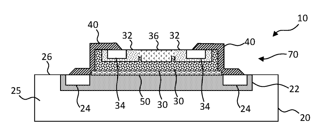
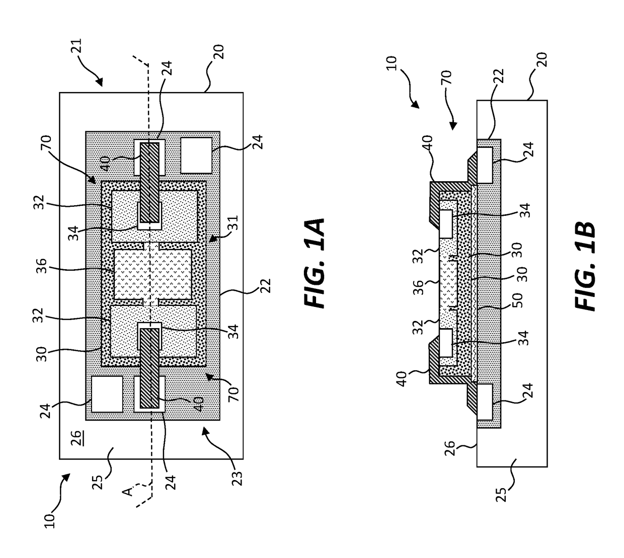
[0069]Referring to the schematic plan view of FIG. 1A and the schematic cross section of FIG. 1B taken across cross section line A of FIG. 1A, in an embodiment of the present invention, a compound sensor device 10 includes a semiconductor substrate 20. An active electronic circuit 22 is formed in or on the semiconductor substrate 20, for example, using photolithographic methods found in the integrated circuit industry. The active electronic circuit 22 can be, for example, a circuit for controlling a sensor 70, sending or receiving signals to or from the sensor 70, or processing signals received from the sensor 70. The active electronic circuit 22 can also send and receive signals to and from an external device (not shown). The active electronic circuit 22 includes two or more circuit connection pads 24 connected to the active electronic circuit 22 for providing signals to the active electronic circuit 22 or receiving signals from the active electronic circuit 22. The sensor 70 is re...


PUM

PropertyMeasurementUnit
lengthaaaaaaaaaa
lengthaaaaaaaaaa
lengthaaaaaaaaaa

Abstract

A compound sensor device includes a semiconductor substrate having an active electronic circuit formed in or on the semiconductor substrate. A sensor comprising a sensor substrate including a sensor circuit having an environmental sensor or actuator formed in or on the sensor substrate is micro-transfer printed onto the semiconductor substrate. One or more electrical conductors electrically connects the active electronic circuit to the sensor circuit. The semiconductor substrate comprises a first material and the sensor substrate comprises a second material different from the first material.

Description

PRIORITY APPLICATIONS[0001]This application claims priority to U.S. Provisional Patent Application No. 62 / 291,830, filed Feb. 5, 2016, entitled Micro-Transfer-Printed Compound Sensor Device, and to U.S. Provisional Patent Application No. 62 / 293,612, filed Feb. 10, 2016, entitled Micro-Transfer-Printed Compound Sensor Device, the contents of all of which are hereby incorporated by reference in their entirety.CROSS REFERENCE TO RELATED APPLICATION[0002]This application is related to U.S. patent application Ser. No. 15 / 047,250 filed Feb. 18, 2016, entitled Micro-Transfer-Printed Acoustic Wave Filter Device, and to U.S. patent application Ser. No. 15 / 048,134, filed Feb. 19, 2016, entitled Compound Micro-Transfer-Printed Optical Filter Device, and to G.B. patent application Ser. No. 1419515.0 filed Nov. 3, 2014, entitled Magnetic Field Sensor and Method of Making Same, the contents of all of which are hereby incorporated by reference in their entirety.FIELD OF THE INVENTION[0003]The pres...

Claims


Application Information

Patent Timeline
Patent Type & Authority Applications(United States)
IPC IPC(8): B81B7/00B81C3/00
CPCB81B7/0077B81C3/001B81C2203/0792B81C2203/032B81B2207/012B81C1/00373B81C2201/0194B81C2203/051
Inventor COK, RONALD S.
Owner X CELEPRINT LIMITED
Why Eureka
Try Eureka