Illumination Systems and Methods for Photoluminescence Imaging of Photovoltaic Cells and Wafers

a photovoltaic cell and photoluminescence imaging technology, applied in the field of illumination systems, can solve the problems of significant light safety issues in the prior art laser-based pl imaging system, extreme intensity of image formed on the retina, and short measurement time, so as to improve the thermal emission of the wafer or cell, the effect of shortening the measurement time and high intensity illumination

Inactive Publication Date: 2013-03-14
BT IMAGING PTY LTD
View PDF6 Cites 30 Cited by
  • Summary
  • Abstract
  • Description
  • Claims
  • Application Information

AI Technical Summary

Benefits of technology

[0013]The use of high intensity illumination for generating photoluminescence provides significant advantages in terms of time and cost. For example, flash lamp equipment is generally cheaper than laser light sources and if applied correctly, can provide sufficient energy to produce a photoluminescence effect within a very short space of time, up to 100 milliseconds preferably up to 10 and most preferably a few milliseconds as compared with conventional laser based PL imaging systems.
[0045]This is a particularly useful process when using a silicon CCD sensor. Using an InGaAs camera also allows a shorter measurement time, but it measures longer wavelengths than a Si CCD camera and is therefore relatively more sensitive to thermal emissions from the wafer or cell.

Problems solved by technology

As mentioned above, the laser-based PL imaging systems of the prior art have significant light safety issues.
The potential hazard of laser light sources, and of illumination systems incorporating them, arises from the fact that they may be much brighter than other light sources, where the brightness (in units of power per unit area per unit solid angle) may be defined for example as the optical power passing through an aperture (e.g. a laser output aperture) divided by the aperture area divided by the solid angle subtended by the optical beam in the far field.
When an extremely bright light source is viewed with the eye, either directly or via intermediate optics such as a collimating lens, the image formed on the retina can be extremely intense, resulting in virtually instantaneous and permanent damage.
However although there is less likelihood of this occurring with near IR light from non-laser sources, e.g. from high power LEDs, and the regulatory requirements are less onerous, it needs to be understood that because brightness is a key parameter, light safety issues cannot simply be ignored just because a system uses non-laser light sources.

Method used


Image

  • Illumination Systems and Methods for Photoluminescence Imaging of Photovoltaic Cells and Wafers
  • Illumination Systems and Methods for Photoluminescence Imaging of Photovoltaic Cells and Wafers
  • Illumination Systems and Methods for Photoluminescence Imaging of Photovoltaic Cells and Wafers

Examples


Embodiment Construction

[0058]Preferred embodiments of the invention will now be described, by way of example only, with reference to the accompanying drawings.

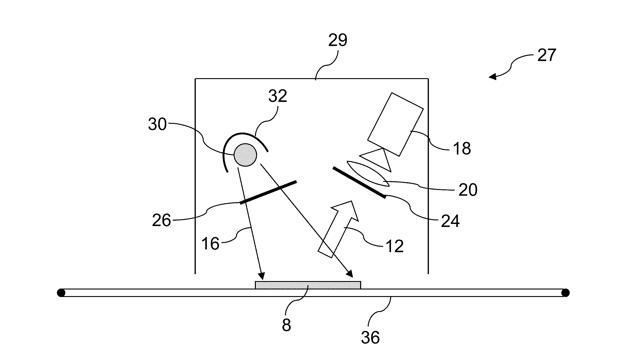
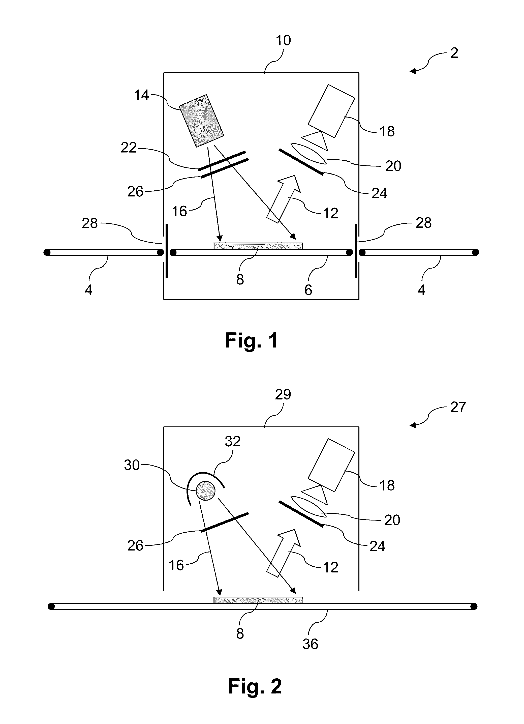
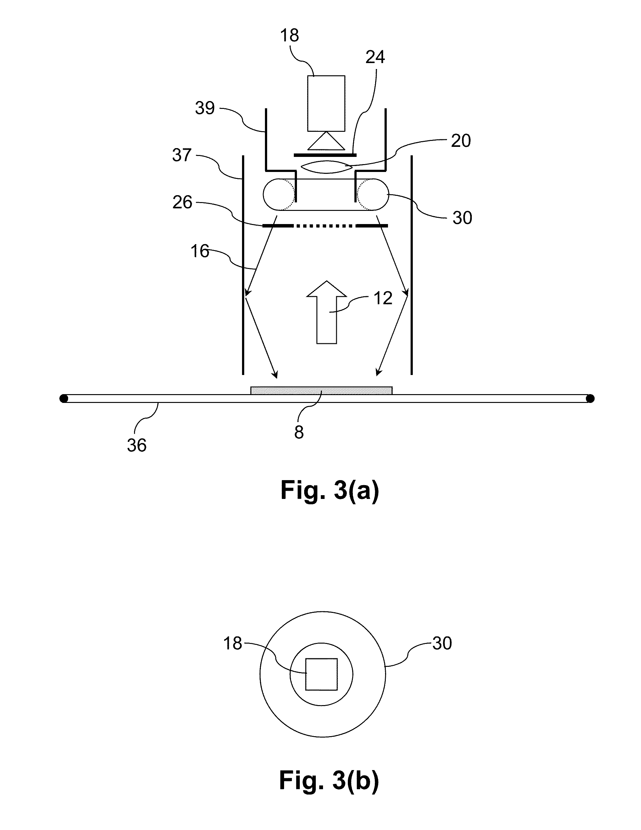
[0059]Photoluminescence (PL) imaging is known to be a rapid and convenient technique for characterising silicon ingots, blocks, wafers, as well as silicon-based photovoltaic (PV) cells both during and after manufacture, using systems and methods described in the abovementioned published PCT patent application No WO 07 / 041,758 A1. The PL emission from silicon arises primarily from band-to-band recombination in the wavelength range 900 to 1300 nm, and can provide information on many material, mechanical and electrical parameters of relevance to PV cell performance including minority carrier diffusion length and minority carrier lifetime, and the impact of certain materials impurities and defects on the these properties.

[0060]FIG. 1 shows a PL imaging system 2 suitable for acquiring PL images of semiconductor devices such as silicon PV cells during the...


PUM

PropertyMeasurementUnit
temperatureaaaaaaaaaa
capture timeaaaaaaaaaa

Abstract

Methods are presented for analysing semiconductor materials (8), and silicon photovoltaic cells and cell precursors in particular, using imaging of photoluminescence (12) generated with high intensity illumination (16). The high photoluminescence signal levels (16) obtained with such illumination (30) enable the acquisition of images from moving samples with minimal blurring. Certain material defects of interest to semiconductor device manufacturers, especially cracks, appear sharper under high intensity illumination. In certain embodiments images of photoluminescence generated with high and low intensity illumination are compared to highlight selected material properties or defects.

Description

FIELD OF THE INVENTION[0001]The present invention relates to illumination systems, and methods using these systems, for the characterisation of semiconductor materials using photoluminescence imaging. The illumination systems have particular application to the characterisation of silicon-based photovoltaic cells and cell precursors.RELATED APPLICATIONS[0002]The present application claims priority from Australian provisional patent application Nos 2010900018, 2010903050 and 2010903975, the contents of which are incorporated herein by reference.BACKGROUND OF THE INVENTION[0003]Any discussion of the prior art throughout this specification should in no way be considered as an admission that such prior art is widely known or forms part of the common general knowledge in the field.[0004]The semiconductor industry has for decades used photoluminescence (PL), the generation of luminescence with above band gap excitation, as a non-destructive method for investigating direct band gap semicond...

Claims


Application Information

Patent Timeline
Patent Type & Authority Applications(United States)
IPC IPC(8): G01N21/956G01N21/64
CPCG01N21/6489G01N21/9501G01N2201/06113G01N2201/062G01N2201/08
Inventor BARDOS, ROBERT A.WEBER, JUERGENTRUPKE, THORSTENMAXWELL, IAN A.MCMILLAN, WAYNE
Owner BT IMAGING PTY LTD
Why Eureka
Try Eureka