Luminous element for backlight unit

a backlight unit and luminous element technology, applied in the field of luminous elements, can solve the problems of increasing the cost caused by the addition of circuit boards, complicated assembly process, and increasing processing time and cost, so as to reduce manufacturing process and cost, minimize substrate size, and minimize the size of backlight units

Inactive Publication Date: 2012-12-25
SEOUL SEMICONDUCTOR
View PDF18 Cites 0 Cited by
  • Summary
  • Abstract
  • Description
  • Claims
  • Application Information

AI Technical Summary

Benefits of technology

[0011]The present invention is conceived to solve the aforementioned problems. Accordingly, an object of the present invention is to provide a luminous element for a backlight unit, in which luminous chips are arranged on a substrate so that manufacturing time and cost can be reduced.
[0012]Another object of the present invention is to provide a luminous element for a backlight unit, in which the size of a backlight unit can be minimized by minimizing the size of a substrate when manufacturing the luminous element
[0013]A further object of the present invention is to provide a luminous element for a backlight unit, in which the viewing angle of the luminous element is optimized thus to increase the luminance uniformity of a liquid crystal display.
[0018]As described above, the present invention provides a luminous element for a backlight unit, in which luminous chips are arranged on a substrate so that the manufacturing process and cost can be reduced and the size of a substrate is minimized when manufacturing the luminous element, thereby minimizing the size of a backlight unit.
[0019]Further, the present invention provides a luminous element for a backlight unit, in which luminance uniformity can be increased by optimizing the viewing angle of the luminous element.

Problems solved by technology

However, in the aforementioned conventional structure, an assembling process is complicated and difficult, and the processing time and cost are required to mount the separately manufactured luminous elements on a substrate.
That is, since a substrate having luminous chips mounted thereon and the luminous element including the luminous chips mounted on the substrate should be arranged on a separately prepared circuit board, the cost caused from the addition of the circuit board is increased.
Further, the additional circuit board requires a space for positioning the luminous elements.
Accordingly, there is a problem in that the entire size of a backlight unit is increased.

Method used


Image

  • Luminous element for backlight unit
  • Luminous element for backlight unit

Examples


Embodiment Construction

[0022]Hereinafter, a preferred embodiment of the present invention will be described in detail with reference to the accompanying drawings.

[0023]However, the present invention is not limited to the embodiment disclosed herein but may be embodied in different forms. The embodiment is provided only for illustrative purposes and for full understanding of the scope of the present invention by those skilled in the art. Throughout the drawings, like reference numerals are used to designate like elements.

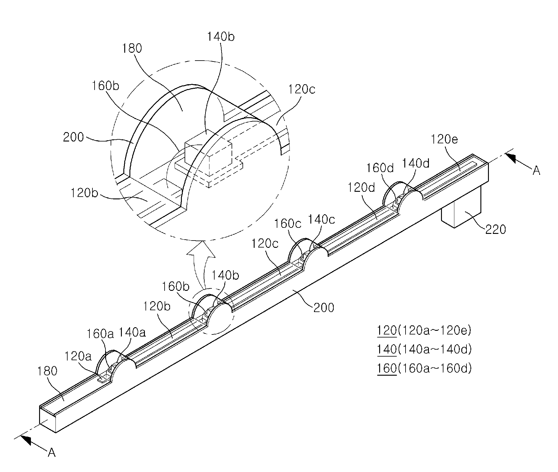
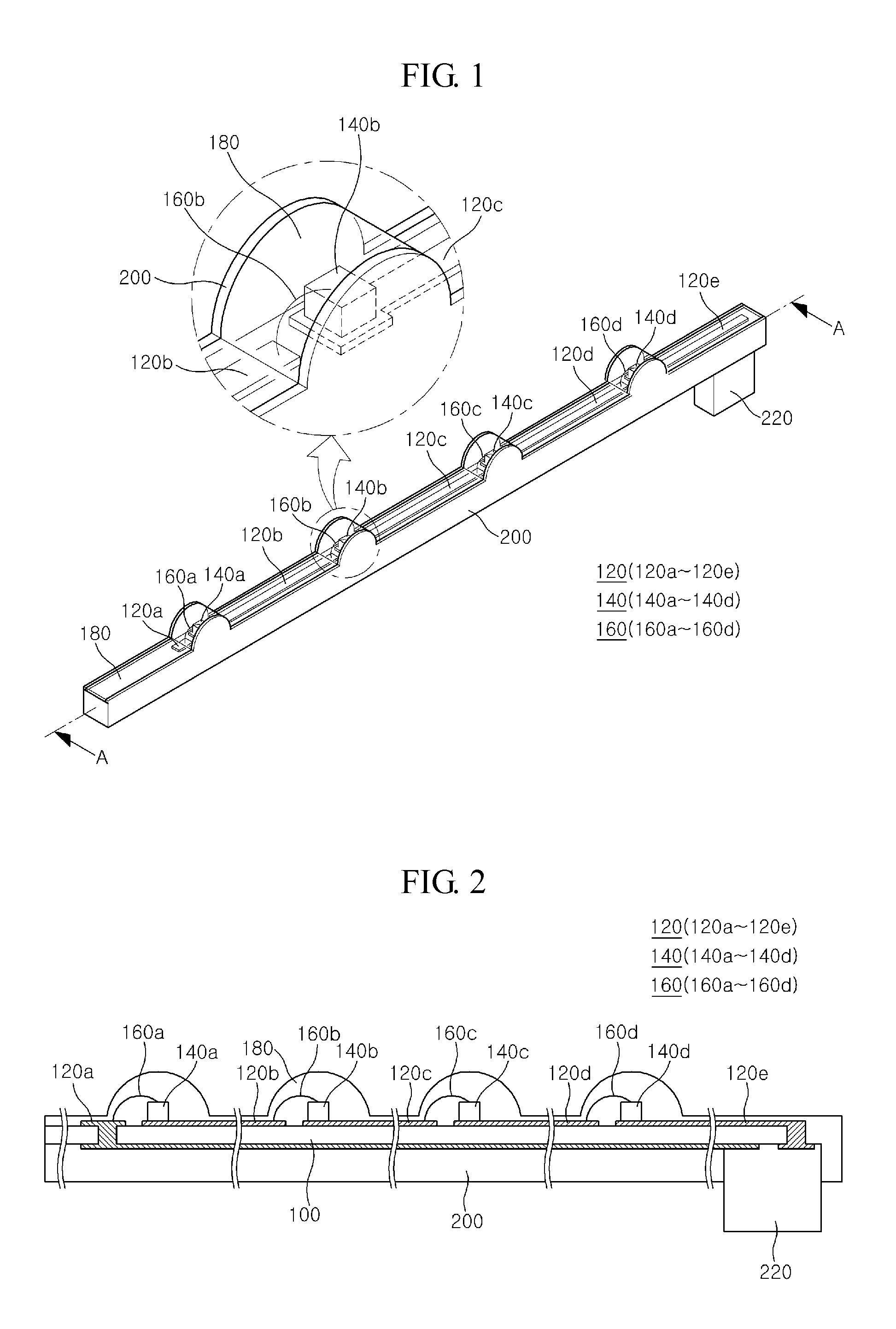
[0024]FIG. 1 is a perspective view of a luminous element for a backlight unit according to the present invention, and FIG. 2 is a sectional view taken along line A-A in FIG. 1.

[0025]The luminous element for a backlight unit according to the present invention will be described with reference toFIGS. 1 and 2. The luminous element for a backlight unit includes a substrate 100, an electrode pattern 120 formed on top and bottom surfaces of the substrate 100, luminous chips 140 mounted on the el...


PUM


Abstract

The present invention relates to a luminous element, and more particularly, to a luminous element for a backlight unit with a plurality of luminous chips mounted on a substrate. The present invention provides a luminous element for a backlight unit, in which luminous chips are arranged on a substrate so that the manufacturing process and cost can be reduced and the size of a substrate is minimized when manufacturing the luminous element, thereby minimizing the size of a backlight unit. Further, the present invention provides a luminous element for a backlight unit, in which luminance uniformity can be increased by optimizing the viewing angle of the luminous element.

Description

CROSS REFERENCE RELATED APPLICATIONS[0001]This application is the National Stage of International Application No. PCT / KR2006 / 004859, filed Nov. 17, 2006, and claims priority from and the benefit of Korean Patent Application No. 10-2005-0110713, filed on Nov. 18, 2005, which are both hereby incorporated by reference for all purposes as if fully set forth herein.BACKGROUND OF THE INVENTION[0002]1. Field of the Invention[0003]The present invention relates to a luminous element, and more particularly, to a luminous element for a backlight unit with a plurality of luminous chips mounted on a substrate.[0004]2. Discussion of the Background[0005]In general, the application range of a liquid crystal displays (LCD) has extended because of its lightweight, thin, low-power drive, full color and high resolution characteristics. A liquid crystal display has been currently used in a computer, notebook computer, PDA, telephone, TV, audio / video device or the like. In such a liquid crystal display, ...

Claims


Application Information

Patent Timeline
Patent Type & Authority Patents(United States)
IPC IPC(8): F21S4/00F21V1/00
CPCG02F1/133608G02F1/133606H01L33/486H01L33/60F21S4/003F21Y2101/02H01L2224/48091H01L2224/48227H01L2924/00014F21S4/20F21Y2115/10G02F1/1335
Inventor RYU, SEUNG RYEOLKANG, SEOK JIN
Owner SEOUL SEMICONDUCTOR
Why Eureka
Try Eureka