Semiconductor device having a nonvolatile memory cell with a cap insulating film formed over a selection gate electrode

a nonvolatile memory cell and non-volatile technology, applied in the field of semiconductor devices, can solve the problems of monos type non-volatile memory cells with various technical problems, all charges stored in storage nodes leak out, etc., and achieve the effect of suppressing the reduction of drive force and improving reliability

Inactive Publication Date: 2013-01-01
RENESAS ELECTRONICS CORP
View PDF45 Cites 8 Cited by
  • Summary
  • Abstract
  • Description
  • Claims
  • Application Information

AI Technical Summary

Benefits of technology

[0006]Because of the above, a MONOS type nonvolatile memory cell which uses a nitride film as a charge storage layer attracts attention recently. In this case, it is possible to improve the reliability of data retention because charges contributing to data storage are stored in discrete traps of a nitride film, which is an insulator, and therefore, it is unlikely that all charges in the charge storage layer leak out even if an abnormal leak occurs owing to the occurrence of a defect in some part of an oxide film surrounding the storage node.
[0014]The present invention provides a technique capable of suppressing the reduction of the drive force and of improving reliability of a semiconductor device having a nonvolatile memory cell.
[0021]It is possible to improve reliability by suppressing the reduction of the drive force in a semiconductor device having a non-volatile memory cell.

Problems solved by technology

However, with an EEPROM having such a structure, there may be a case where all charges stored in a storage node leak out owing to abnormal leakage if there occurs a defect in some part of an oxide film that surrounds the floating gate electrode because the charge storage layer is a conductor.
However, the MONOS type nonvolatile memory cell has various technical problems as described below.

Method used


Image

  • Semiconductor device having a nonvolatile memory cell with a cap insulating film formed over a selection gate electrode
  • Semiconductor device having a nonvolatile memory cell with a cap insulating film formed over a selection gate electrode
  • Semiconductor device having a nonvolatile memory cell with a cap insulating film formed over a selection gate electrode

Examples


first embodiment

(First Embodiment)

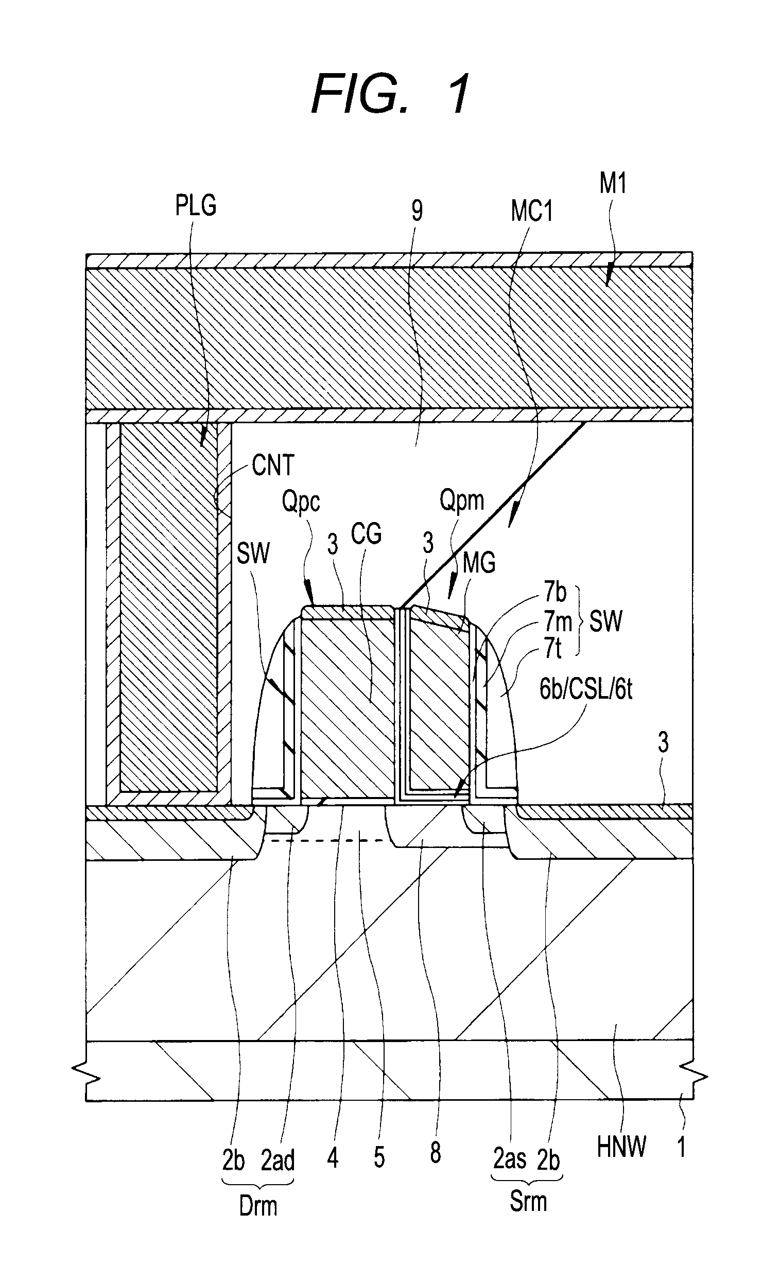
[0057]An example of a structure of a nonvolatile memory cell according to a first embodiment will be explained by using FIG. 1. FIG. 1 is a section view of essential parts of a nonvolatile memory cell obtained by cutting a channel along a direction that intersects a memory gate electrode, showing an example of a MONOS type nonvolatile memory cell with a split gate structure in which a memory gate electrode in the form of a sidewall is formed over one side surface of a selection pMIS selection gate electrode.

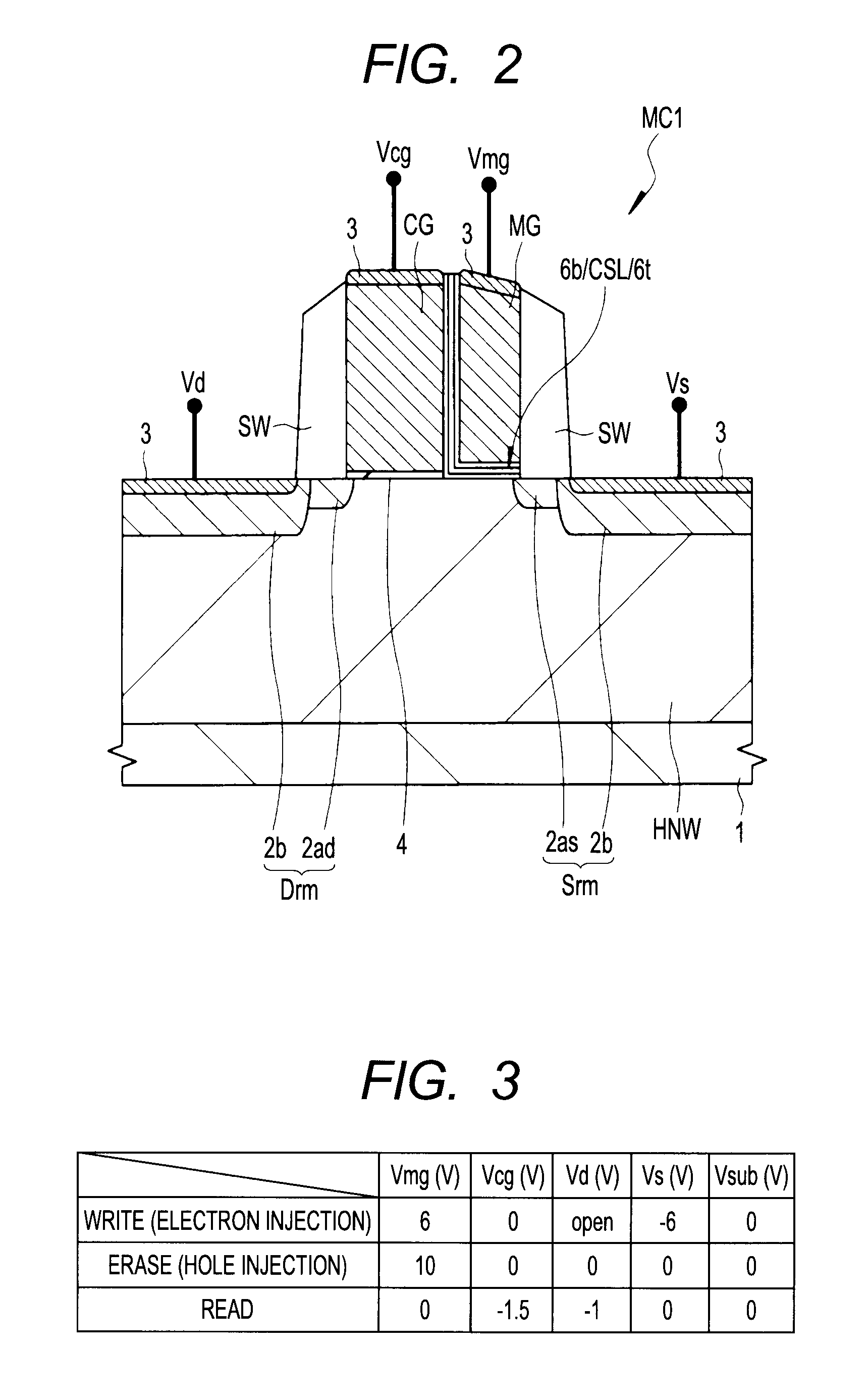
[0058]As shown in FIG. 1, a semiconductor substrate 1 includes, for example, p-type single crystal silicon and on the side of its main surface (device formation surface), an n-type well HNW is formed. Consequently, the semiconductor substrate 1 in the region where a memory cell MC1 is formed exhibits an n-type conductivity. Further, in the active region of the main surface of the semiconductor substrate 1, a selection pMIS (Qpc) and a memory pMIS (Qpm) of the me...

second embodiment

(Second Embodiment)

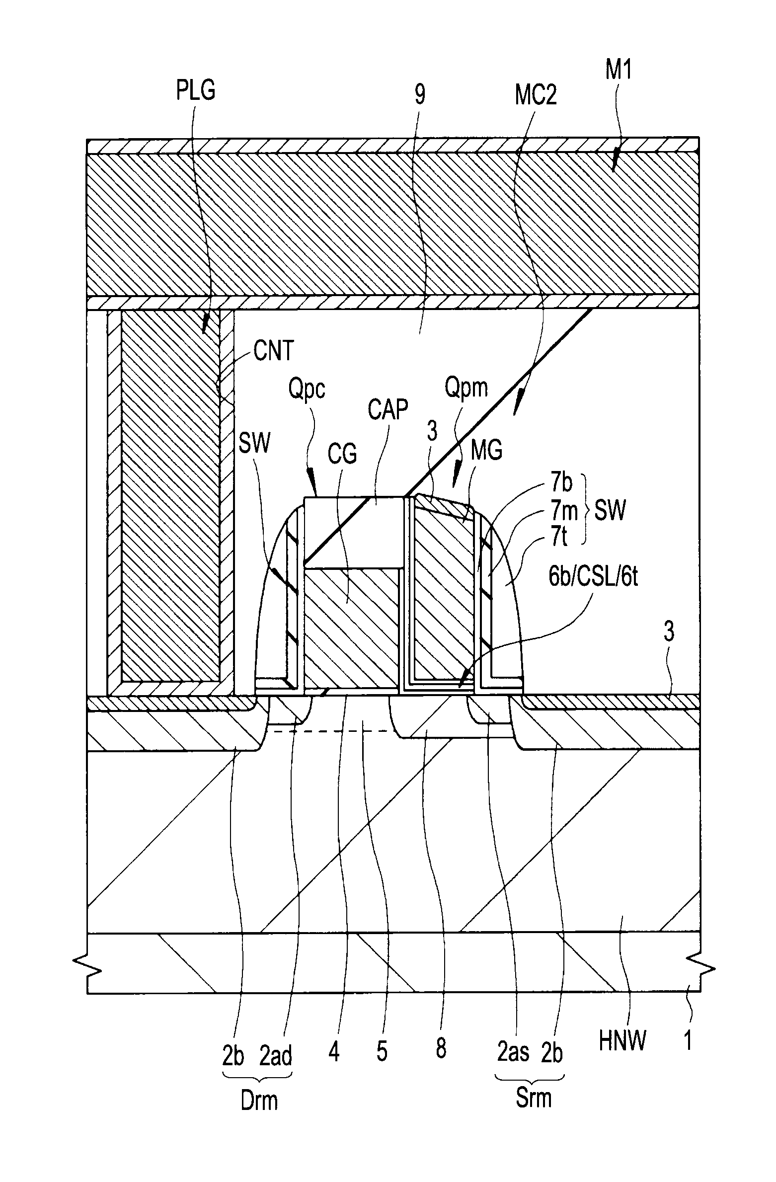
[0081]In a second embodiment, as in the first embodiment described above, a MONOS type nonvolatile memory cell with a split gate structure is used as a p-type memory cell including the selection pMIS (Qpc) and the memory pMIS (Qpm). A difference from the first embodiment described above lies in fact that a cap insulating film (CAP) is formed over the top surface of the selection gate electrode CG of the selection pMIS (Qpc). By the cap insulating film (CAP), it is possible to cause compression stress to occur in the channel region (between the source region Srm and the drain region Drm) under the selection gate electrode CG. The p-type memory cell uses holes the mobility of which is lower than that of electrons at the time of read, and therefore, there is a possibility that the operation speed may be reduced compared to the n-type memory cell. Because of this, the cap insulating film is formed over the top surface of the selection gate electrode CG and compression...

third embodiment

(Third Embodiment)

[0132]In a third embodiment, as in the second embodiment described above, a MONOS type nonvolatile memory cell with a split gate structure is used as a p-type memory cell including the selection pMIS (Qpc) and the memory pMIS (Qpm), and over the top surface of the selection gate electrode CG of the selection pMIS (Qpc), the cap insulating film CAP is formed, which causes compression stress to occur, in the channel region (between the source region Srm and the drain region Drm) under the selection gate electrode CG. A difference from the second embodiment described above lies in the fact that an insulating film having compression stress is formed over the p-type memory cell formed in the memory region and over the low voltage system pMIS and the high voltage system pMIS formed in the peripheral circuit region, and an insulating film having tensile stress is formed over the low voltage system nMIS and the high voltage system nMIS formed in the peripheral circuit regi...


PUM


Abstract

To provide a technique capable of improving reliability of a semiconductor device having a nonvolatile memory cell by suppressing the reduction of the drive force.A memory cell is configured by a selection pMIS having a selection gate electrode including a conductive film exhibiting a p-type conductivity and a memory pMIS having a memory gate electrode including a conductive film exhibiting a p-type conductivity, and at the time of write, hot electrons are injected into a charge storage layer from the side of a semiconductor substrate 1 and at the time of erase, hot holes are injected into the charge storage layer from the memory gate electrode.

Description

CROSS-REFERENCE TO RELATED APPLICATION[0001]The disclosure of Japanese Patent Application No. 2009-27604 filed on Feb. 9, 2009 including the specification, drawings and abstract is incorporated herein by reference in its entirety.BACKGROUND OF THE INVENTION[0002]The present invention relates to a semiconductor device and its manufacturing technique, in particular, to technology which is effective when applied to a semiconductor device having a MONOS (Metal Oxide Nitride Oxide Semiconductor) type nonvolatile memory cell and its manufacturing.[0003]For example, in the twelfth embodiment of Japanese Patent Laid-Open No. 2004-303918 (Patent Document 1), a nonvolatile memory cell is disclosed, in which the erase speed is increased by constituting a memory gate electrode by a two-layer conductive layer and making the concentration of n-type impurity in the lower conductive layer lower than the concentration of n-type impurity in the upper conductive layer, and then erasing data by utilizi...

Claims


Application Information

Patent Timeline
Patent Type & Authority Patents(United States)
IPC IPC(8): H01L29/792
CPCH01L21/28282H01L27/105H01L27/11568H01L27/11573H01L29/66833H01L29/792H01L29/40117H10B43/30H10B43/40
Inventor KAWASHIMA, YOSHIYUKIHARAGUCHI, KEIICHI
Owner RENESAS ELECTRONICS CORP
Why Eureka
Try Eureka