Encapsulated MEMS device and method to form the same

a technology of mems and encapsulation, applied in the field of microelectromechanical systems (mems), can solve the problems of loss of freedom of movement during operation, many devices, especially mems devices, and complex manufacturing process

Active Publication Date: 2013-01-08
SEMICON MFG INT (SHANGHAI) CORP
View PDF40 Cites 128 Cited by
  • Summary
  • Abstract
  • Description
  • Claims
  • Application Information

AI Technical Summary

Problems solved by technology

Furthermore, consistency requirements for the performance of MEMS devices (both intra-device and device-to-device) often dictate that the processes used to fabricate such MEMS devices need to be extremely sophisticated.
Many devices, particularly MEMS devices, do not function properly when embedded in a completely solid environment.
Freedom to move during operation would be lost if these elements were simply left embedded in a solid film deposited over the substrate, as is commonly done in the microelectronics industry.
However, a released micromechanical structure is fragile and must be protected with some form of package which isolates a microenvironment surrounding the micromechanical structure from a global environment surrounding the substrate.
However, this type of packaging is not wafer-level and is limited to stand-alone (discrete) devices, and therefore is expensive.

Method used


Image

  • Encapsulated MEMS device and method to form the same
  • Encapsulated MEMS device and method to form the same
  • Encapsulated MEMS device and method to form the same

Examples


Embodiment Construction

[0015]An encapsulated MEMS device and a method to form an encapsulated MEMS device are described. In the following description, numerous specific details are set forth, such as material compositions and chemical regimes, in order to provide a thorough understanding of the present invention. It will be apparent to one skilled in the art that the present invention may be practiced without these specific details. In other instances, well-known features such as lithographic parameters and patterning procedures are not described in detail in order to not unnecessarily obscure the present invention. Furthermore, it is to be understood that the various embodiments shown in the Figures are illustrative representations and are not necessarily drawn to scale.

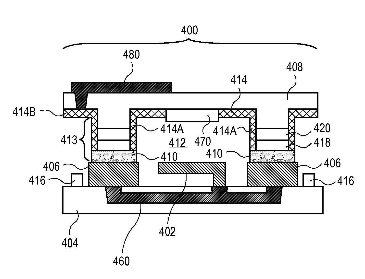
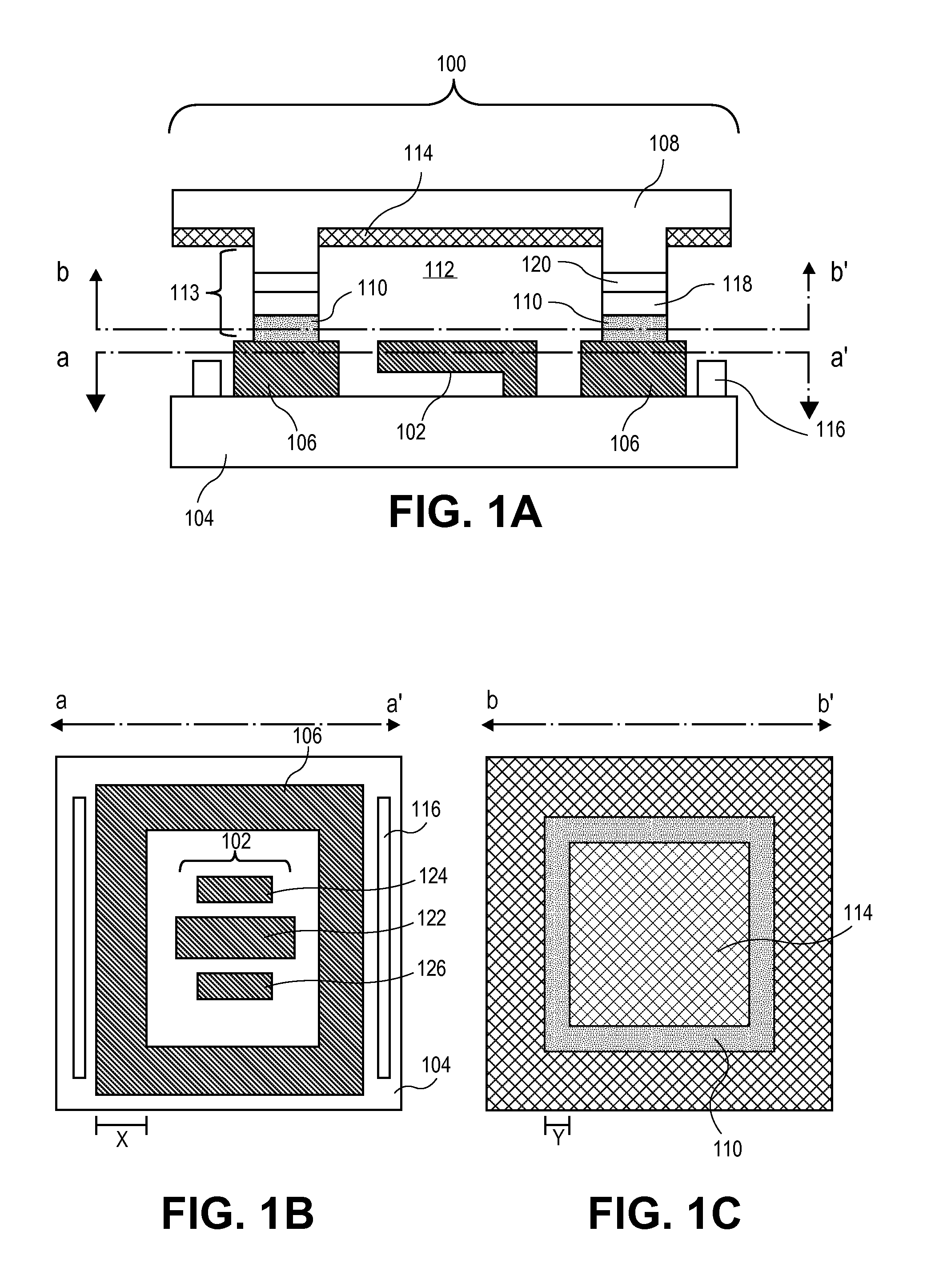
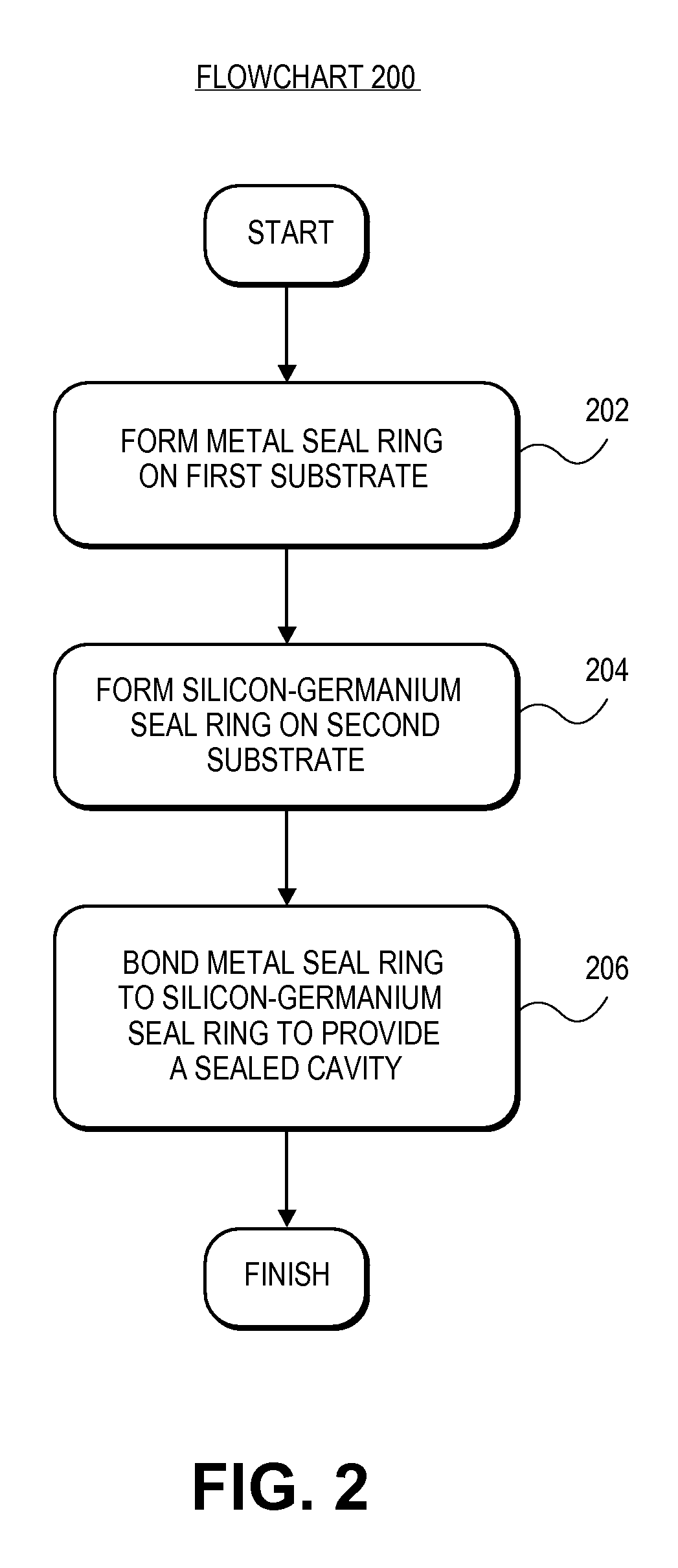
[0016]Disclosed herein are an encapsulated MEMS device and a method to form an encapsulated MEMS device. An apparatus may include a first substrate having a silicon-germanium seal ring disposed thereon and a second substrate having a meta...


PUM


Abstract

An encapsulated MEMS device and a method to form an encapsulated MEMS device are described. An apparatus includes a first substrate having a silicon-germanium seal ring disposed thereon and a second substrate having a metal seal ring disposed thereon. The metal seal ring is aligned with and bonded to the silicon-germanium seal ring to provide a sealed cavity. A MEMS device is housed in the sealed cavity. A method includes forming a silicon-germanium seal ring on a first substrate and forming a metal seal ring on a second substrate. The metal seal ring is bonded to the silicon-germanium seal ring to provide a sealed cavity that houses a MEMS device.

Description

BACKGROUND OF THE INVENTION[0001]1) Field of the Invention[0002]The invention is in the field of Microelectromechanical Systems (MEMS).[0003]2) Description of Related Art[0004]For the past several years, MEMS structures have been playing an increasingly important role in consumer products. For example, MEMS devices, such as sensors, detectors and mirrors, can be found in products ranging from air-bag triggers in vehicles to displays in the visual arts industry. In another example, high quality MEMS oscillators may be used in place of crystal oscillators to keep track of time and to provide a stable clock signal for digital integrated circuits. As these technologies mature, the demands on precision and functionality of the MEMS structures have escalated. For example, optimal performance may depend on the ability to fine-tune the characteristics of various components of these MEMS structures. Furthermore, consistency requirements for the performance of MEMS devices (both intra-device ...

Claims


Application Information

Patent Timeline
Patent Type & Authority Patents(United States)
IPC IPC(8): H01L29/84
CPCG01L9/0019G01C19/5783B81B7/0038B81B7/0064G01P2015/088
Inventor GAN, QINGQUEVY, EMMANUEL P.
Owner SEMICON MFG INT (SHANGHAI) CORP
Why Eureka
Try Eureka