Supercharge Your Innovation With Domain-Expert AI Agents!

Production method for laminated electronic component

a production method and electronic component technology, applied in the direction of fixed capacitor details, variable capacitors, stacked capacitors, etc., can solve the problems of reduced measurement accuracy and cumbersome operation, and achieve the effect of accurately measuring the side gap and minimizing the size of the electronic componen

Active Publication Date: 2013-02-26
MURATA MFG CO LTD
View PDF25 Cites 0 Cited by
  • Summary
  • Abstract
  • Description
  • Claims
  • Application Information

AI Technical Summary

Benefits of technology

[0009]To overcome the problems described above, preferred embodiments of the present invention provide a production method for a laminated electronic component, which can accurately measure the side gap between an end surface of a ceramic base body and an internal electrode and which can minimize the size of the electronic component.
[0011]In the above-described production method for the laminated electronic component, external terminal electrodes are formed on the first side surface of the ceramic base body by plating. Since the plating grows substantially equally from the centers of the exposed portions of the internal electrodes to the right and left, it can be determined whether or not the side gap is sufficient while the distance between the external terminal electrodes and the first end surface of the ceramic base body is replaced with the actual side gap. Since the external terminal electrode is observed as one surface, it is easily recognized as an image, and this allows the distance to be accurately measured.
[0013]According to a preferred embodiment of the present invention, it is possible to easily and accurately measure the side gap, to efficiently remove defective ceramic base bodies, and to design the side gap to have as small a value as possible. Therefore, the size of ceramic base body is prevented from being increased. Furthermore, since the side gap can be measured not only from the side of the first side surface, but also from the side of the first or second principal surface, the degree of flexibility in the measurement direction increases, and measurement can be simultaneously performed on the first and second side surfaces when performed from the side of the principal surface.

Problems solved by technology

This may cause failure, such as a short circuit.
Even if design dimensions are determined in view of the limit of the side gap, since a production process for the capacitor array includes other factors causing failure, such as layer misalignment or displacement due to cutting, the side gap is typically not provided specifically as designed.
Unfortunately, since the exposed portions are relatively small, measurement accuracy is reduced, and the operation is quite cumbersome.

Method used


Image

  • Production method for laminated electronic component
  • Production method for laminated electronic component
  • Production method for laminated electronic component

Examples


first preferred embodiment

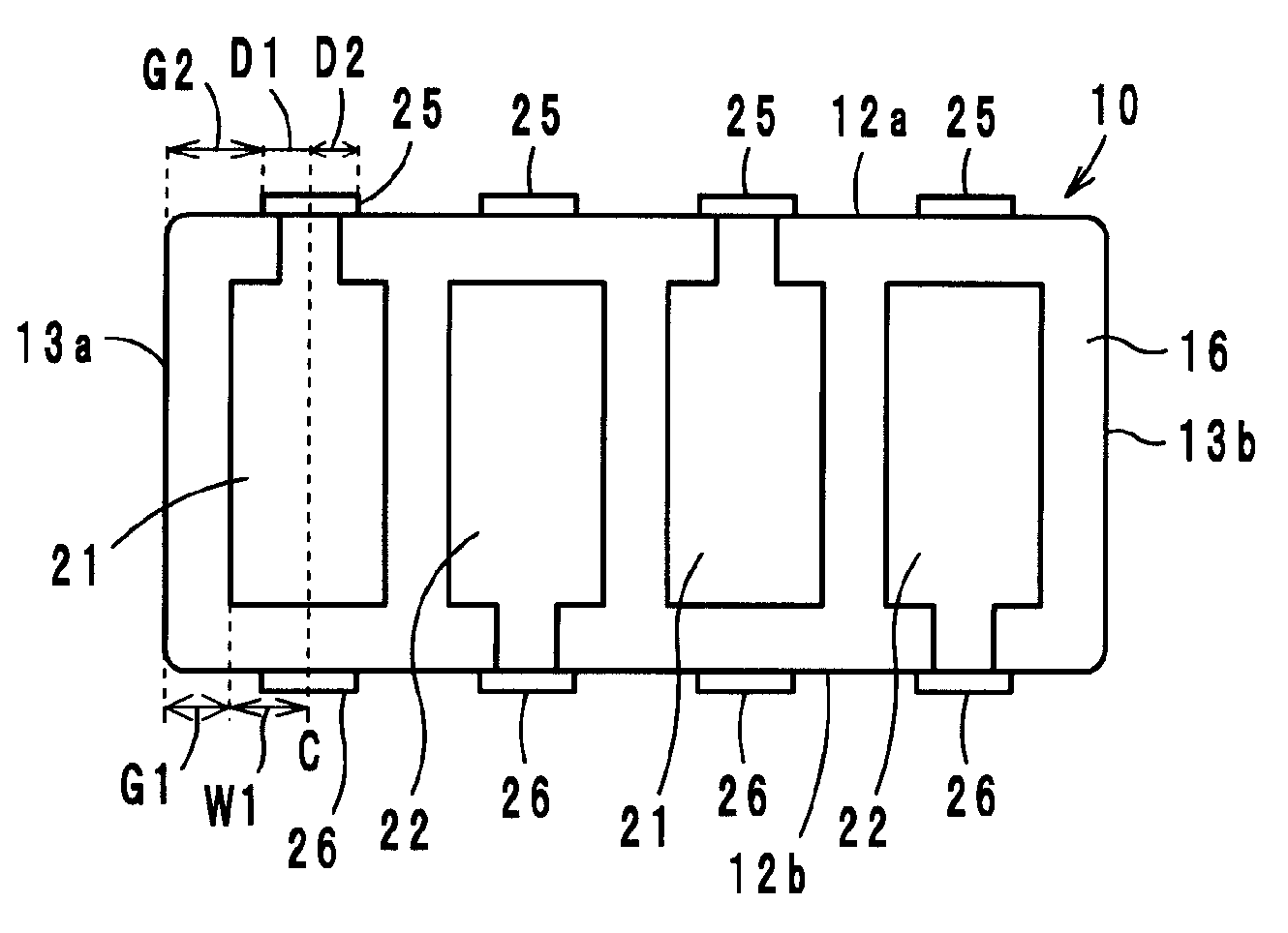
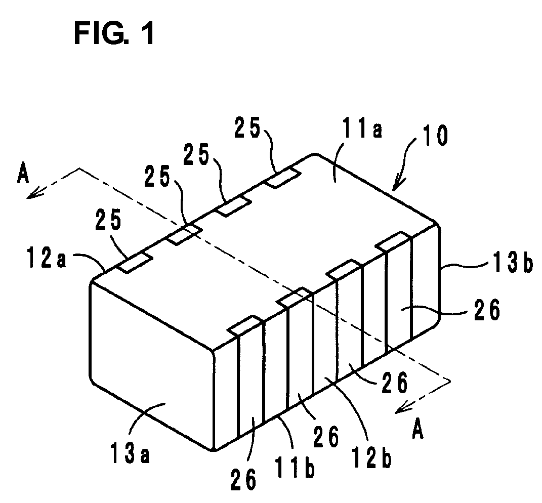
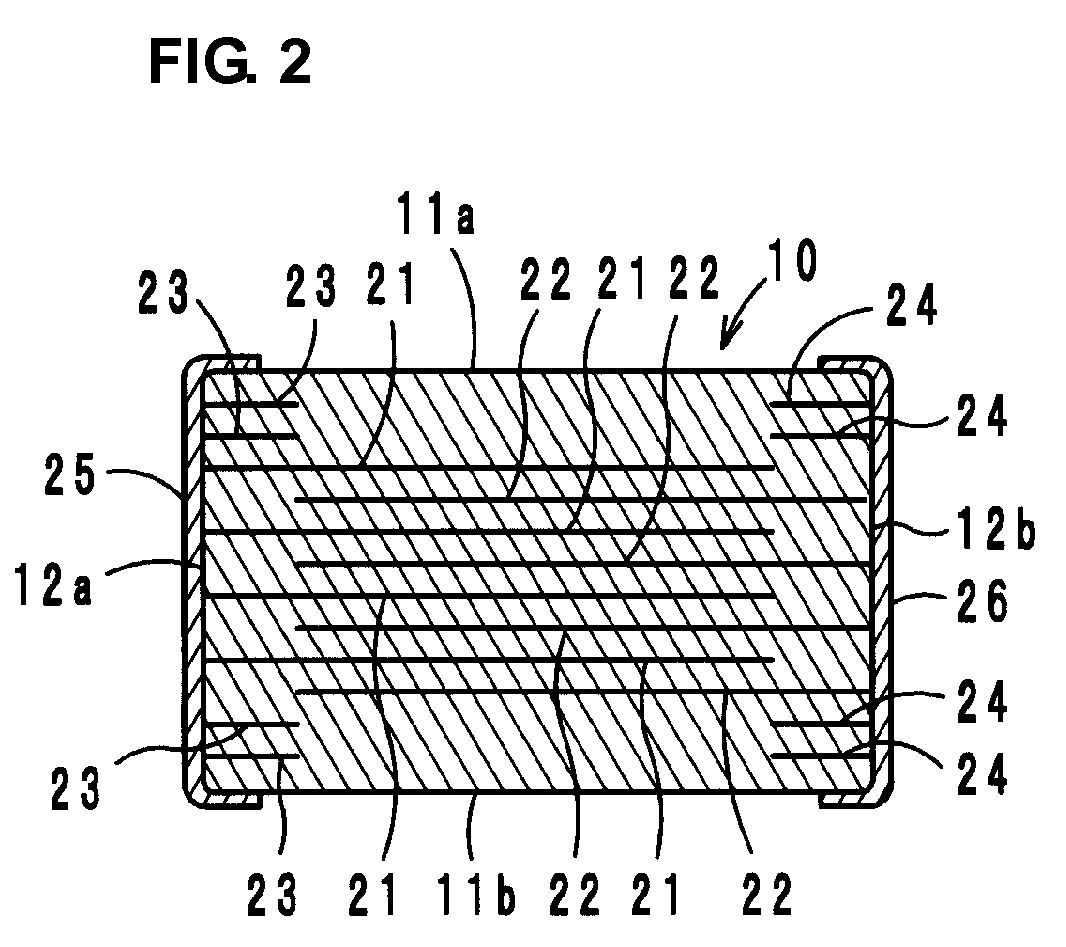
[0025]A description will now be provided of a laminated ceramic capacitor array produced according to a first preferred embodiment of the present invention. Referring to FIGS. 1 to 3, the laminated ceramic capacitor array includes a ceramic base body 10 formed by stacking a plurality of ceramic layers 14 to 19, and first and second internal electrodes 21 and 22 and first and second internal conductors 23 and 24 provided in the ceramic base body 10.

[0026]The ceramic base body 10 has a substantially rectangular parallelepiped shape including first and second opposing principal surfaces 11a and 11b, first and second opposing side surfaces 12a and 12b, and first and second opposing end surfaces 13a and 13b. On the first and second side surfaces 12a and 12b, first external terminal electrodes 25, and second external terminal electrodes 26 are provided, respectively. Each of the first and second external terminal electrodes 25 and 26 are shaped substantially like a vertically extending be...

second preferred embodiment

[0055]FIG. 7 shows two ceramic layers in a low-ESL multiterminal laminated ceramic capacitor according to a second preferred embodiment of the present invention. In this laminated ceramic capacitor, first and second internal electrodes 21 and 22 are provided with a plurality of lead-out portions having exposed portions. The exposed portions of the first and second internal electrodes 21 and 22 are offset from each other on first and second side surfaces 12a and 12b of a base body 10. In this laminated ceramic capacitor, the side gap G1 can also be determined by forming external terminal electrodes 25 and 26 on the first and second side surfaces 12a and 12b by plating and measuring the distance G2 from the external terminal electrodes 25 and 26 to end surfaces 13a and 13b of the base body 10.

third preferred embodiment

[0056]FIG. 8 shows two ceramic layers in a two-terminal laminated ceramic capacitor according to a third preferred embodiment of the present invention. In this laminated ceramic capacitor, first and second internal electrodes 21 and 22 have long exposed portions, and first and second external terminals 25 and 26 having relatively large areas are provided on first and second side surfaces 12a and 12b of a base body 10. In this laminated ceramic capacitor, the side gap G1 can also be determined by forming the external terminal electrodes 25 and 26 on the side surfaces 12a and 12b by plating and measuring the distance G2 from the external terminal electrodes 25 and 26 to end surfaces 13a and 13b of the base body 10.


PUM


Abstract

In a production method for a laminated electronic component, a ceramic base body is formed by stacking a plurality of ceramic layers, and internal electrodes are formed in the ceramic base body. Lead-out portions of the internal electrodes are exposed from side surfaces of the ceramic base body. Belt-shaped external terminal electrodes are formed on the side surfaces by plating so as to be electrically connected to the exposed portions of the internal electrodes. The distance from an end surface to an external terminal electrode closest to the end surface in the ceramic base body is measured. When the measured distance does not correspond to a predetermined reference value, the ceramic base body is removed as being defective.

Description

BACKGROUND OF THE INVENTION[0001]1. Field of the Invention[0002]The present invention relates to a production method for a laminated electronic component, and more particularly, to a production method for a laminated electronic component, such as a laminated ceramic capacitor array, in which a plurality of internal electrodes are provided between a plurality of ceramic layers.[0003]2. Description of the Related Art[0004]With recent size reduction of electronic apparatuses, such as mobile telephones and portable music players, the mounting density of electronic components on wiring boards included in the electronic apparatuses is increasing rapidly. In response to this, in order to reduce the mounting space and the number of components to be mounted, there is a demand for electronic components to include a plurality of circuit elements in one chip. As such electronic components, array type electronic components represented by a capacitor array are used.[0005]An array type multitermin...

Claims


Application Information

Patent Timeline
Patent Type & Authority Patents(United States)
IPC IPC(8): B05D5/12H01G7/00
CPCH01G4/012H01G4/232H01G4/30Y10T29/435Y10T29/43
Inventor SAKANAKA, ATSUSHI
Owner MURATA MFG CO LTD
Features
  • R&D
  • Intellectual Property
  • Life Sciences
  • Materials
  • Tech Scout
  • Unparalleled Data Quality
  • Higher Quality Content
  • 60% Fewer Hallucinations
Learn More