Multi-chip package having a stacked plurality of different sized semiconductor chips, and method of manufacturing the same

a technology of semiconductor chips and stacked chips, which is applied in the direction of semiconductor devices, semiconductor/solid-state device details, electrical apparatus, etc., can solve the problems of not being able to manufacture mcp at wafer level, and reducing the size of semiconductor chip packages

Active Publication Date: 2013-03-12
SAMSUNG ELECTRONICS CO LTD
View PDF19 Cites 51 Cited by
  • Summary
  • Abstract
  • Description
  • Claims
  • Application Information

AI Technical Summary

Problems solved by technology

Therefore, semiconductor chip packages, which may be considered the core component of an electronic device, are also getting smaller and lighter.
The MCP may be stacked with different types of semiconductor chips, each of the semiconductor chips having different sizes; therefore, it is not possible to manufacture the MCP at a wafer level.

Method used


Image

  • Multi-chip package having a stacked plurality of different sized semiconductor chips, and method of manufacturing the same
  • Multi-chip package having a stacked plurality of different sized semiconductor chips, and method of manufacturing the same
  • Multi-chip package having a stacked plurality of different sized semiconductor chips, and method of manufacturing the same

Examples


Embodiment Construction

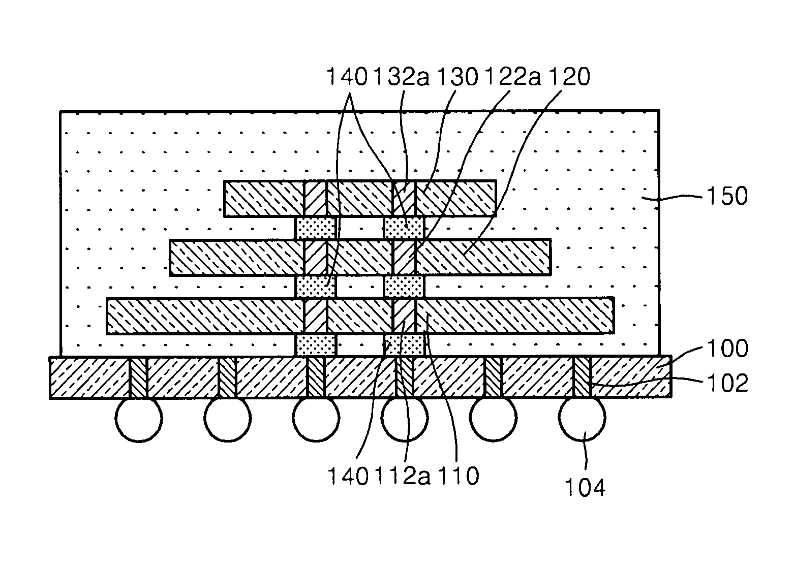
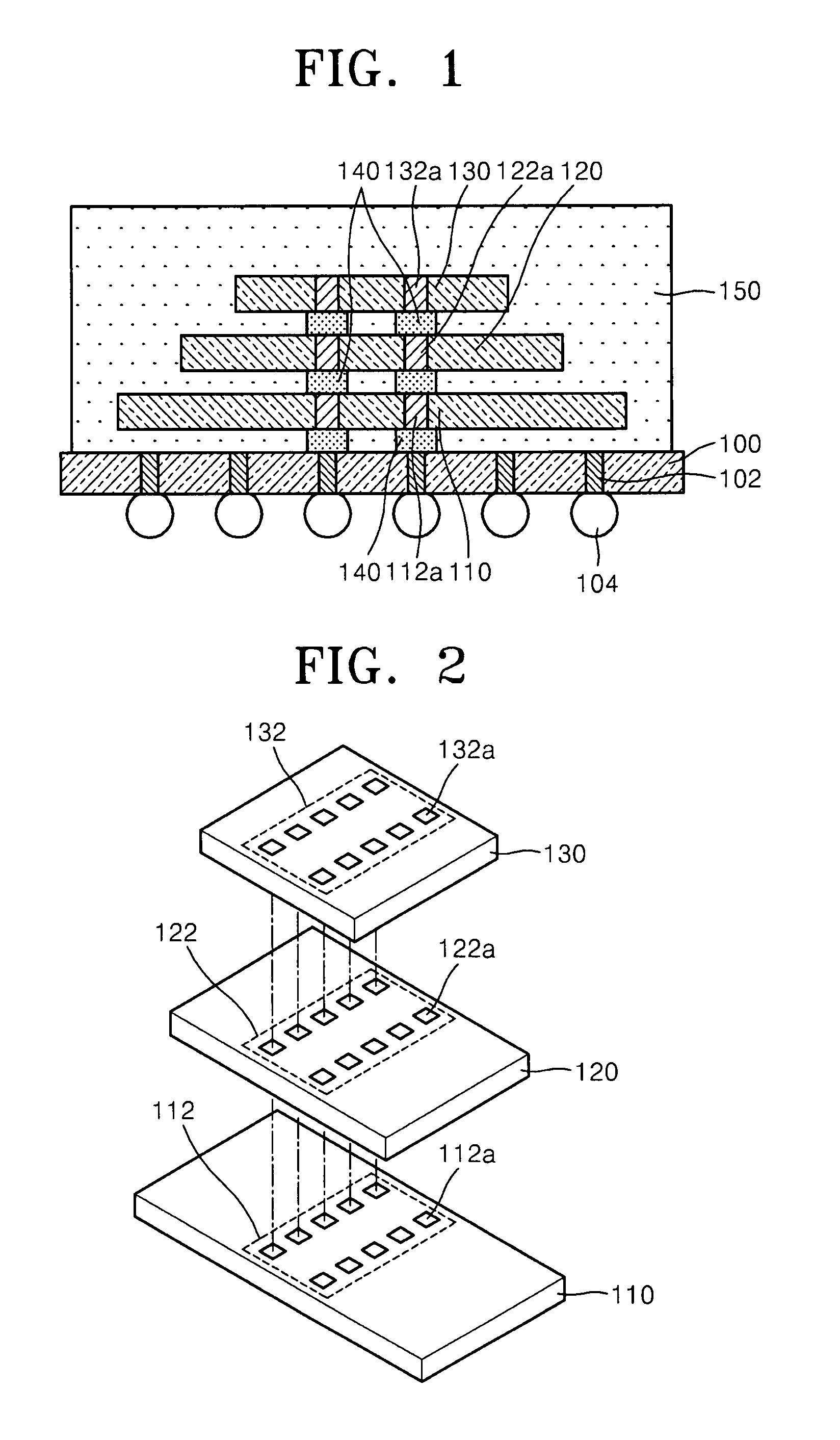
[0026]It will be understood that when an element or layer is referred to as being “on”, “connected to” or “coupled to” another element or layer, it may be directly on, connected or coupled to the other element or layer or intervening elements or layers may be present. In contrast, when an element is referred to as being “directly on,”“directly connected to” or “directly coupled to” another element or layer, there may be no intervening elements or layers present. As used herein, the term “and / or” includes any and all combinations of one or more of the associated listed items.

[0027]It will be understood that, although the terms first, second, third, etc. may be used herein to describe various elements, components, regions, layers and / or sections, these elements, components, regions, layers and / or sections should not be limited by these terms. These terms may be only used to distinguish one element, component, region, layer or section from another region, layer or section. Thus, a firs...


PUM


Abstract

Provided is a multi-chip package in which a plurality of semiconductor chips having different sizes are stacked. A multi-chip package may include a substrate, and a plurality of semiconductor chips stacked on the substrate, each of the plurality of semiconductor chips having a different size. Each of the plurality of semiconductor chips including a pad group and a reference region associated with the pad group, each pad group having a plurality of pads, and the plurality of pads in each pad group located at same coordinates with respect to the associated reference region, and each of the plurality of semiconductor chips having their reference regions vertically aligned.

Description

PRIORITY CLAIM[0001]A claim of priority is made to Korean Patent Application No. 10-2006-0074658, filed on Aug. 8, 2006, in the Korean Intellectual Property Office, the disclosure of which is incorporated herein in its entirety by reference.BACKGROUND[0002]1. Field of the Invention[0003]Example embodiments of the present invention may relate to a multi-chip package, and more particularly, to a multi-chip package having a stacked plurality of different sized semiconductor chips.[0004]2. Description of the Related Art[0005]In response to recent developments in the semiconductor industry and increased user demands, electronic devices are getting smaller and lighter. Therefore, semiconductor chip packages, which may be considered the core component of an electronic device, are also getting smaller and lighter. In this regard, a stacked chip package, in which a plurality of semiconductor chips are vertically stacked on a mounting substrate, and a wafer level package, in which semiconduct...

Claims


Application Information

Patent Timeline
Patent Type & Authority Patents(United States)
IPC IPC(8): H01L23/48
CPCH01L21/76898H01L24/06H01L24/17H01L24/73H01L25/0657H01L25/50H01L23/3128H01L23/49816H01L23/49811H01L24/13H01L2224/0401H01L24/81H01L24/85H01L2224/06155H01L2224/06156H01L2224/06165H01L2224/13099H01L2224/16145H01L2224/16237H01L2224/32145H01L2224/48091H01L2224/48227H01L2224/73257H01L2224/81801H01L2224/9202H01L2225/0651H01L2225/06513H01L2225/06517H01L2225/06527H01L2225/06541H01L2225/06551H01L2225/06555H01L2225/06562H01L2225/06586H01L2924/01015H01L2924/01074H01L2924/01082H01L2924/15311H01L2224/73204H01L2224/32225H01L2224/13025H01L24/48H01L2924/01006H01L2924/01033H01L2924/01047H01L2924/014H01L2224/85H01L2224/45139H01L2924/00014H01L2924/00H01L2924/12042H01L24/45H01L2924/181H01L2224/16225H01L2224/16146H01L2224/17181H01L2924/00011H01L2224/45099H01L2224/05599H01L2924/00012H01L2224/45015H01L2924/207H01L2924/01049H01L23/12H01L23/3142H01L23/49827
Inventor EUN, HYUNG-IAE
Owner SAMSUNG ELECTRONICS CO LTD
Why Eureka
Try Eureka