Scalable memory system

a memory system and scalable technology, applied in the field of memory systems, can solve the problems of power consumption in such a configuration becoming an issue, adversely affecting the performance of the system, and imposing physical performance limitations on flash memory systems b>10/b>

Inactive Publication Date: 2013-03-26
CONVERSANT INTPROP MANAGEMENT INC
View PDF70 Cites 35 Cited by
  • Summary
  • Abstract
  • Description
  • Claims
  • Application Information

AI Technical Summary

Benefits of technology

[0029]In yet another embodiment, the step of powering up includes asserting a control signal at a first time to maintain the memory device in a default state prior to a power transition; transistioning a power level of the memory device from a first level to a second level at a second subsequent time while the control signal is asserted; waiting for a predetermined duration of time to allow the power level to stabilize; and de-asserting the control signal at a third subsequent time for releasing the memory device from the default state thereby preventing accidental program or erase operation in the memory device.

Problems solved by technology

There are specific issues that will adversely impact performance of the system.
The configuration of Flash memory system 10 imposes physical performance limitations.
Power consumption in such a configuration becomes an issue as each signal track between the flash controller and flash memory devices is frequently charged and discharged for signaling.
With increasing system clock frequencies, the power consumption will increase.
There is also a practical limit to the number of memory devices which can be connected in parallel to the channel since the drive capability of a single memory device is small relative to the loading of the long signal tracks.
A controller configured to have multiple channels and additional chip enable signals increases the cost of the memory system.
Otherwise, the memory system is limited to a small number of memory devices.

Method used


Image

  • Scalable memory system
  • Scalable memory system
  • Scalable memory system

Examples


Embodiment Construction

[0060]In the following detailed description of embodiments of the present invention, reference is made to the accompanying drawings which form a part hereof, and in which is shown by way of illustration of specific embodiments in which the present invention may be practiced. These embodiments are described in sufficient detail to enable those of ordinary skill in the art to practice the present invention, and it is to be understood that other embodiments may be utilized and that logical, electrical, and other changes may be made without departing from the scope of the present invention. The following detailed description is, therefore, not to be taken in a limiting sense, and the scope of the present invention is defined by the appended claims.

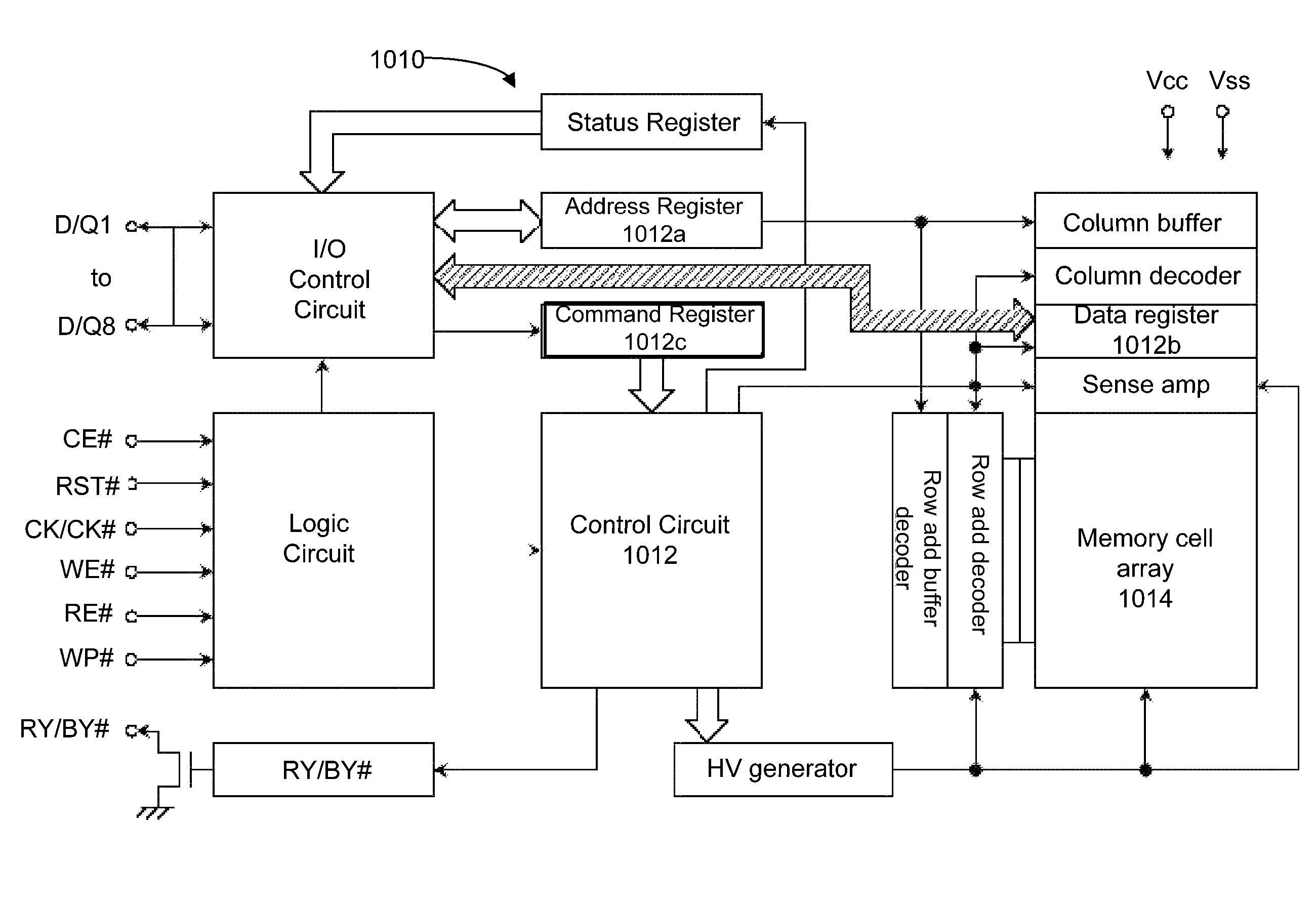
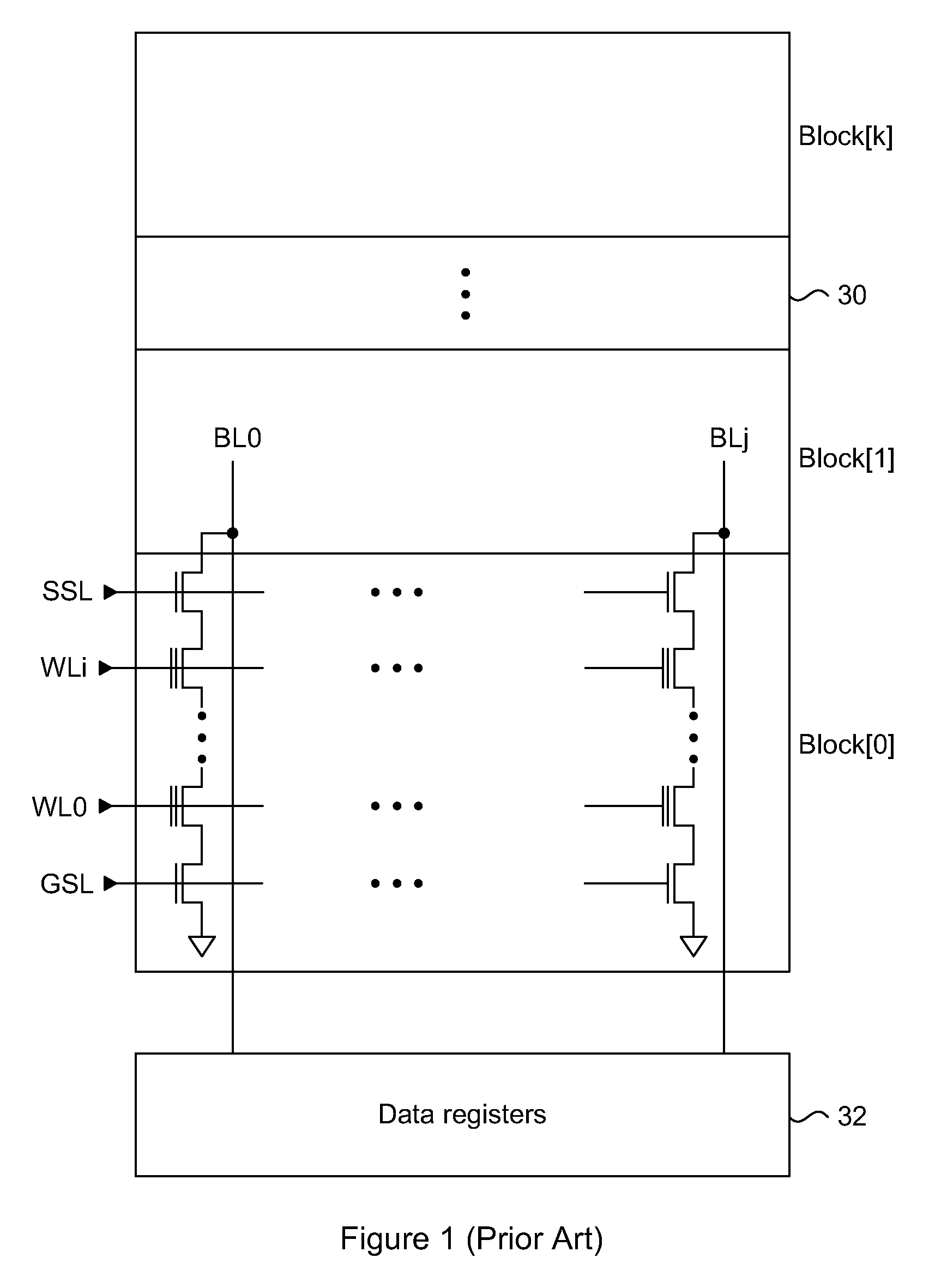
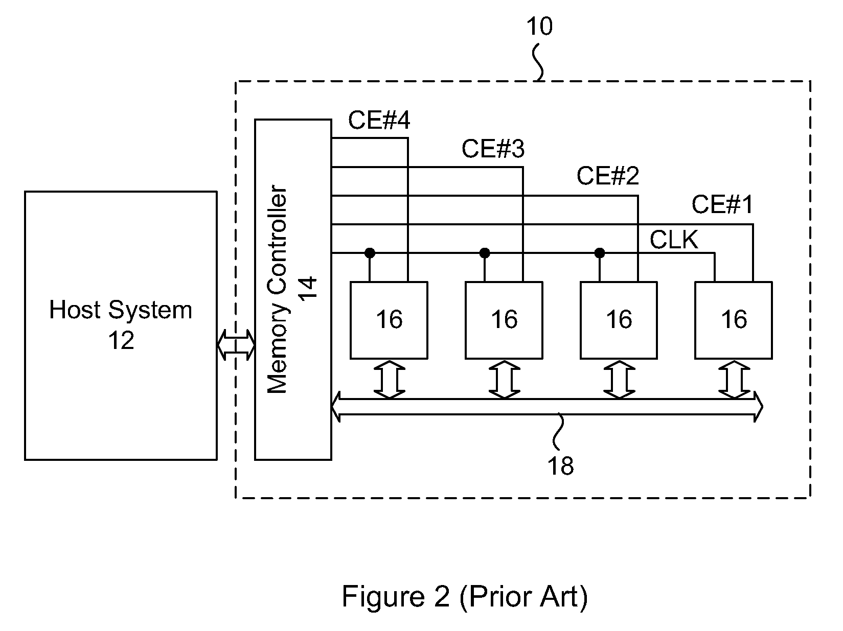
[0061]A memory system architecture having serially connected memory devices is described. The memory system is scalable to include any number of memory devices without any performance degradation or complex redesign. Each memory device has a s...


PUM


Abstract

A memory system architecture has serially connected memory devices. The memory system is scalable to include any number of memory devices without any performance degradation or complex redesign. Each memory device has a serial input / output interface for communicating between other memory devices and a memory controller. The memory controller issues commands in at least one bitstream, where the bitstream follows a modular command protocol. The command includes an operation code with optional address information and a device address, so that only the addressed memory device acts upon the command. Separate data output strobe and command input strobe signals are provided in parallel with each output data stream and input command data stream, respectively, for identifying the type of data and the length of the data. The modular command protocol is used for executing concurrent operations in each memory device to further improve performance.

Description

CROSS REFERENCE TO RELATED APPLICATIONS[0001]This application claims the benefit of priority of U.S. Provisional Patent Application No. 60 / 839,329 filed on Aug. 22, 2006; U.S. Provisional Patent Application No. 60 / 868,773 filed on Dec. 6, 2006; U.S. Provisional Patent Application No. 60 / 902,003 filed on Feb. 16, 2007; and U.S. Provisional Patent Application Ser. No. 60 / 892,705 filed on Mar. 2, 2007, the contents of which are incorporated herein by reference in their entirety.FIELD OF THE INVENTION[0002]The present invention relates generally to memory systems. More particularly, the present invention relates to a memory system of serially connected memory devices for mass storage applications.BACKGROUND OF THE INVENTION[0003]Flash memory is a commonly used type of non-volatile memory in widespread use as mass storage for consumer electronics, such as digital cameras and portable digital music players for example. The density of a presently available Flash memory chip can be up to 32...

Claims


Application Information

Patent Timeline
Patent Type & Authority Patents(United States)
IPC IPC(8): G06F12/00
CPCG06F13/1694G06F13/4256G11C7/10G11C7/22G11C16/10G06F12/0623G11C7/1042G11C16/06Y02B60/1235Y02B60/1228G11C2216/30Y02D10/00
Inventor KIM, JIN-KIOH, HAKJUNEPYEON, HONG BEOMPRZYBYLSKI, STEVEN
Owner CONVERSANT INTPROP MANAGEMENT INC
Why Eureka
Try Eureka