Close-packed array of light emitting devices

a technology of light emitting devices and arrays, which is applied in the direction of semiconductor devices for light sources, lighting and heating apparatus, planar light sources, etc., can solve the problems of led chip failure, reduced light produced by leds and led chip efficiency, and inefficient process of light producing leds. achieve the effect of efficient light production and effective thermal managemen

Active Publication Date: 2013-04-09
UT BATTELLE LLC
View PDF15 Cites 47 Cited by
  • Summary
  • Abstract
  • Description
  • Claims
  • Application Information

AI Technical Summary

Benefits of technology

[0007]A close-packed array of LEDs configured for directional heat dissipation is described here. The flexible design platform may allow for effective thermal management and efficient light production from a large number of closely spaced LEDs.

Problems solved by technology

However, the process of producing light from LEDs may be inefficient, particularly at the power levels needed for practical lighting applications, with a substantial amount of the electrical energy being converted into heat energy.
Because of this temperature increase, the amount of light produced by the LEDs and the efficiency of the LEDs decrease.
If the temperature continues to rise, the LED chip may eventually fail as the actual chip temperature exceeds the maximum junction temperature for the chip.
The heat generated by the LEDs and the risk of failure becomes even more significant when the LEDs are densely concentrated on the chip.
These techniques, however, may cause an undesirable increase in the size and power usage of the LED device, thereby limiting their application.

Method used


Image

  • Close-packed array of light emitting devices
  • Close-packed array of light emitting devices
  • Close-packed array of light emitting devices

Examples


example 1

[0057]The thermal diffusivity of ten glass-tungsten rod composite specimens were measured using a flash diffusivity apparatus. An 8 ms pulse from a 2.4 kW Xe lamp (Acute 2-2400, Profoto) positioned about 300 mm from the specimen was employed for excitation. Heat propagation was monitored on the backside of the specimen using a 2 mm2 In—Sb detector. A 2-mm-thick sample of bulk SiC with a known thermal diffusivity of 0.0354 cm2 / s was used as a calibration standard.

[0058]Referring to Table 1, six of the composite specimens evaluated in the thermal diffusivity experiments include tungsten rods of about 100 microns in diameter, and four of the specimens include tungsten rods of about 75 microns in diameter. The number of conductive rods embedded within each glass matrix ranged from 352 to 982, and the overall diameter of the glass-tungsten rod composites ranged from about 0.4 mm to about 0.7 mm.

[0059]

TABLE 1Results of Thermal Diffusivity ExperimentsResults# ofSampleType%DwireDfiberwiresA...

example 2

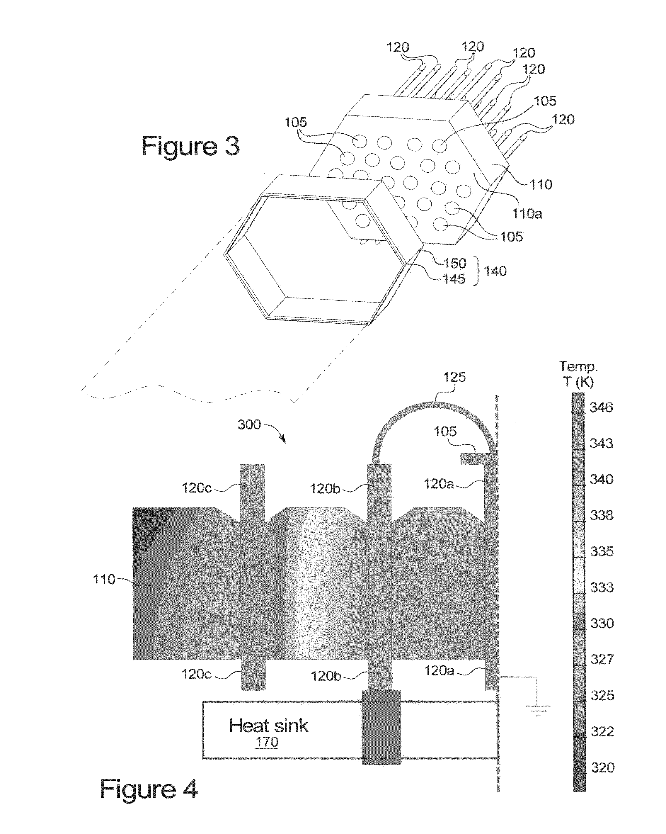
[0061]Near-infrared (NIR) imaging is employed to confirm that tungsten rods embedded in a glass matrix are effective in removing heat anisotropically from an LED. To carry out the imaging experiments, a 2 mm-thick composite of tungsten rods embedded in a glass matrix is irradiated with NIR radiation. Referring to FIG. 12, the tungsten rods are about 100 microns in diameter and are separated by about 100 microns of glass. The conditions of the irradiation are similar to those for the diffusivity experiments, except that the detection is carried out with an InSb NIR camera. Direct imaging of the heat propagation shows that the tungsten rods play the role of heat pipes for longitudinal conduction of heat. The heat removed from an LED may be transferred to a heat sink and / or removed via convection from exposed portions of the rods, as described previously.


PUM


Abstract

A close-packed array of light emitting diodes includes a nonconductive substrate having a plurality of elongate channels extending therethrough from a first side to a second side, where each of the elongate channels in at least a portion of the substrate includes a conductive rod therein. The conductive rods have a density over the substrate of at least about 1,000 rods per square centimeter and include first conductive rods and second conductive rods. The close-packed array further includes a plurality of light emitting diodes on the first side of the substrate, where each light emitting diode is in physical contact with at least one first conductive rod and in electrical contact with at least one second conductive rod.

Description

FEDERALLY SPONSORED RESEARCH OR DEVELOPMENT[0001]This invention was made with government support under Contract No. DE-AC05-00OR22725 awarded by the U.S. Department of Energy. The government has certain rights in the invention.TECHNICAL FIELD[0002]The present disclosure is directed generally to light emitting diodes and more particularly to a close-packed array of such devices.BACKGROUND[0003]A light-emitting diode (LED) is an electronic light source based on a semiconductor diode (p-n junction) that may be used in a variety of applications, including as replacements for traditional light source devices. An LED may include an anode and cathode disposed on a chip of semiconductor material. When a diode is forward biased, charge carriers, including electrons and holes, flow through the semiconductor between the anode and cathode. When electrons and holes recombine, they release energy in the form of a photon. The color of the light corresponds to the energy of the photon, which in tur...

Claims


Application Information

Patent Timeline
Patent Type & Authority Patents(United States)
IPC IPC(8): H01L33/00
CPCH01L25/0753F21V29/80F21K9/56F21Y2101/02F21Y2105/001H01L33/641H01L33/642H01L2224/48091H01L33/647H01L2924/00014H01L2924/00F21Y2105/10F21K9/64F21Y2115/10
Inventor IVANOV, ILIA N.SIMPSON, JOHN T.
Owner UT BATTELLE LLC
Why Eureka
Try Eureka