Methods for pattern matching in a double patterning technology-compliant physical design flow

a technology of physical design flow and pattern matching, applied in the field of method for fabricating an integrated circuit, can solve the problem that eda tools cannot identify all possible decomposition solutions

Inactive Publication Date: 2013-04-09
GLOBALFOUNDRIES INC
View PDF5 Cites 17 Cited by
  • Summary
  • Abstract
  • Description
  • Claims
  • Application Information

AI Technical Summary

Problems solved by technology

However, due to the complexity of mask-layer assignments, cuts, stitch-region generation, and design rule interactions, EDA tools cannot identify all possible decomposition solutions such that DPT-compliance check violations (i.e., f

Method used


Image

  • Methods for pattern matching in a double patterning technology-compliant physical design flow
  • Methods for pattern matching in a double patterning technology-compliant physical design flow
  • Methods for pattern matching in a double patterning technology-compliant physical design flow

Examples


Embodiment Construction

[0019]The following detailed description is merely exemplary in nature and is not intended to limit the invention or the application and uses of the invention. Furthermore, there is no intention to be bound by any expressed or implied theory presented in the preceding technical field, background, brief summary or the following detailed description.

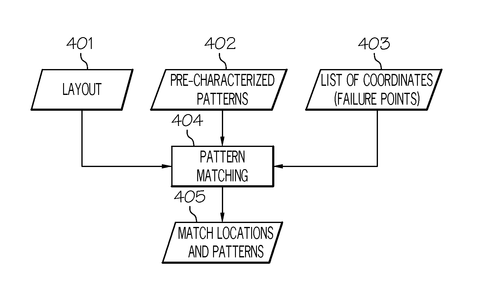
[0020]This disclosure presents a novel methodology employing a library of pre-characterized DPT-compliant patterns and a pattern matching engine that can be used to guide layout designers in resolving DPT-compliant check violations. As such, the methodology presented herein reduces the number of design cycle iterations in the physical design flow used to create double patterning technology (DPT)-compliant logical layout designs. The proposed methodology introduces a pattern matching module that can easily be integrated in the DPT-compliant design flow.

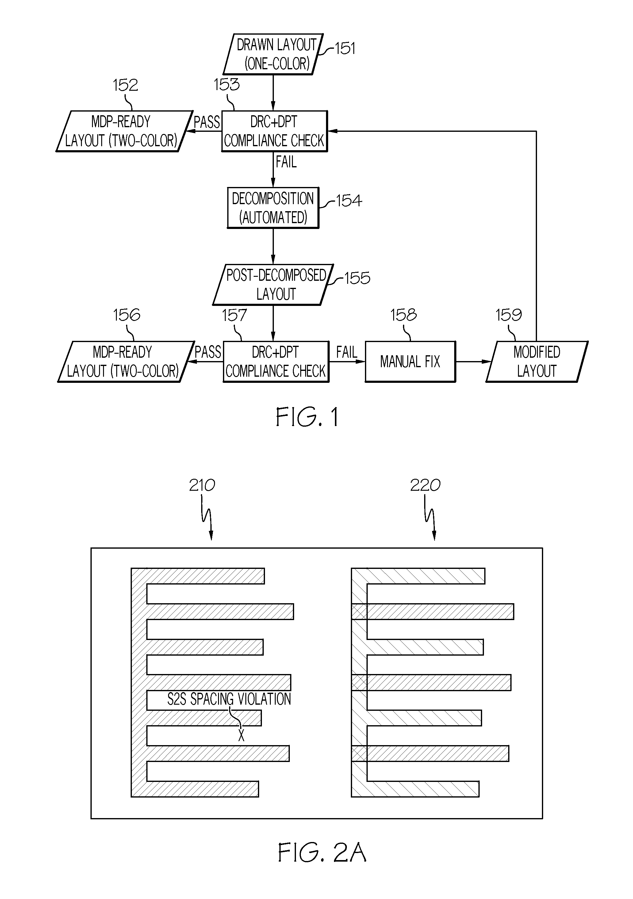
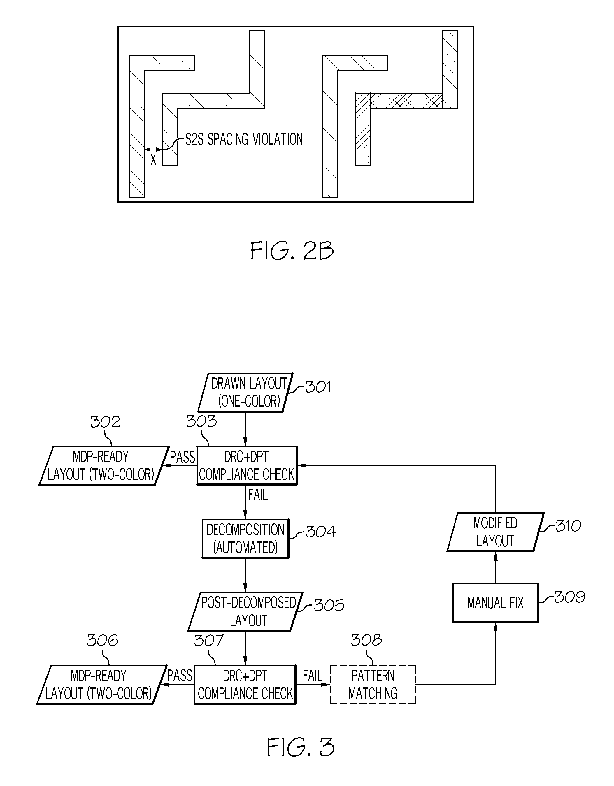
[0021]With reference now to FIG. 3, a novel DPT-compliant methodology integrates pattern ...


PUM


Abstract

A method for fabricating an integrated circuit is disclosed that includes, in accordance with an embodiment, providing a drawn layout logical design for the integrated circuit, the logical design including a plurality of patterns; checking the plurality of patterns for double patterning technology compliance; identifying a non-double patterning technology compliant pattern; providing a double patterning technology compliant pattern for replacing the identified non-double patterning technology compliant pattern, thereby creating a modified logical design; generating a mask set implementing the modified logical design; and employing the mask set to implement the modified logical design in and on a semiconductor substrate.

Description

TECHNICAL FIELD[0001]The present invention generally relates to methods for fabricating an integrated circuit, and more particularly relates to methods that include pattern matching in a double patterning technology-compliant physical design flow.BACKGROUND[0002]There is a continuing trend within the microelectronics industry to incorporate more circuitry having greater complexity on a single integrated circuit (IC) chip. Maintaining this trend generally entails shrinking the size of individual devices within the circuit by reducing the critical dimensions (CDs) of device elements along with the pitch, or the CD of such an element added to the spacing between elements. Microlithography tooling and processing techniques play an important role in resolving the features necessary to fabricate devices and accordingly, are continually under development to meet industry milestones relating to the CD and pitch characteristic of each new technology generation.[0003]High numerical aperture (...

Claims


Application Information

Patent Timeline
IPC IPC(8): G06F17/50
CPCG06F17/5081G06F30/398
Inventor WANG, LYNN T.DAI, VITOCAPODIECI, LUIGI
Owner GLOBALFOUNDRIES INC
Why Eureka
Try Eureka