Photoelectric conversion module for optical communication
a conversion module and optical communication technology, applied in the direction of instruments, optical elements, discharge tubes/lamp details, etc., can solve the problem of increasing the size of the card edge connector
- Summary
- Abstract
- Description
- Claims
- Application Information
AI Technical Summary
Benefits of technology
Problems solved by technology
Method used
Image

Examples
first embodiment
[0067]Photoelectric Conversion Module
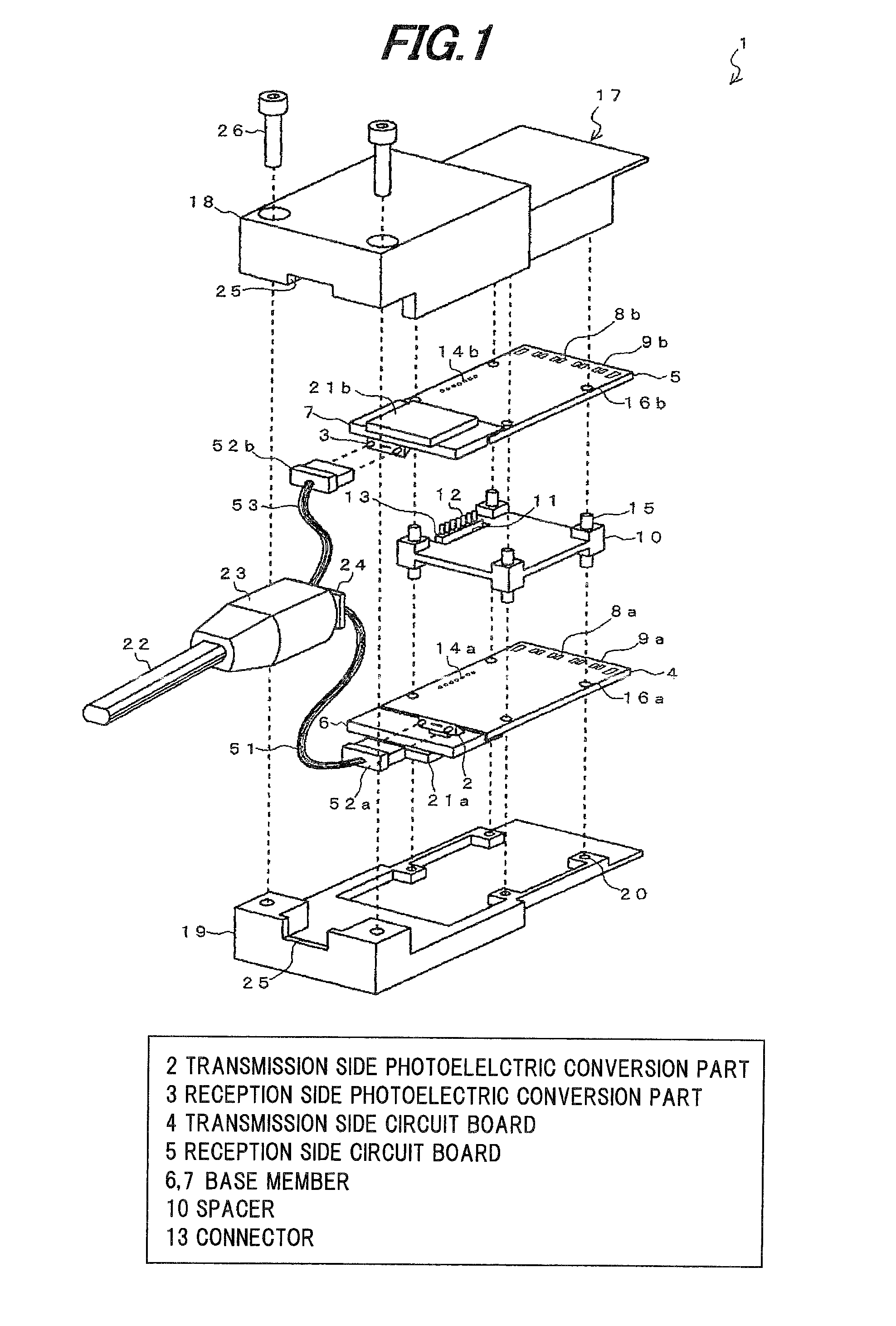
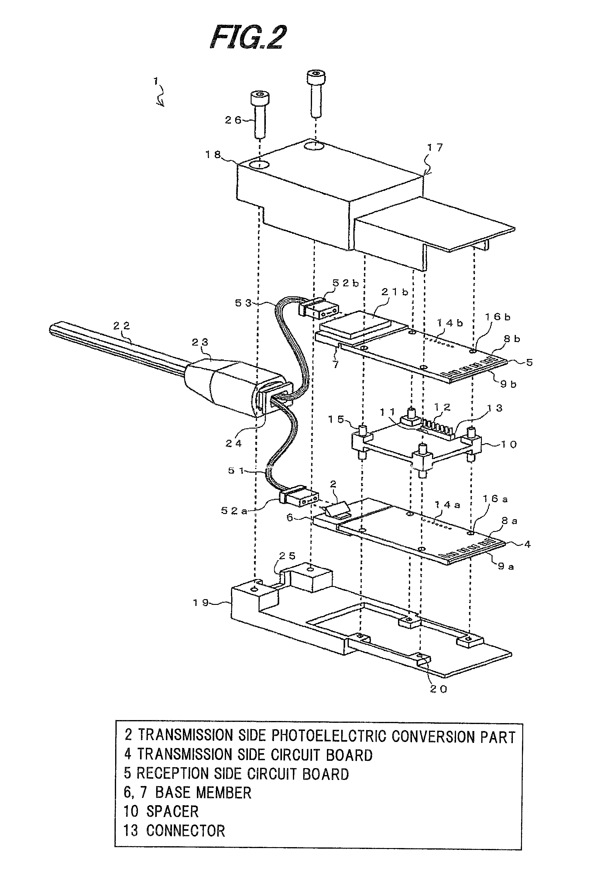
[0068]FIGS. 1 and 2 are exploded perspective views showing a photoelectric conversion module in the first embodiment according to the invention. FIG. 3 is an exploded side view showing the photoelectric conversion module. FIGS. 4A and 4B are perspective views showing the photoelectric conversion module. FIG. 5A is a side view showing the photoelectric conversion module. FIG. 5B is a partial cross sectional view showing the photoelectric conversion module.
[0069]As shown in FIGS. 1 to 5B, the photoelectric conversion module 1 is comprised of a transmission side circuit board 4 in which connecting terminals 8a are formed at one end and a base member 6 with a transmission side photoelectric conversion part 2 mounted thereon is attached at the other end (i.e., at an end opposite to the one end), a reception side circuit board 5 in which connecting terminals 8b are formed at one end and a base member 7 with a reception side photoelectric conversion par...
second embodiment
[0167]The second embodiment according to the invention will be described below.
[0168]FIG. 16A shows the second embodiment of the invention. A photoelectric conversion module 80 in the second embodiment is, like the photoelectric conversion module 1 described above, constructed such that the transmission side circuit board 4 and the reception side circuit board 5 are vertically disposed via the spacer 10 and mounted on the lower housing 19, and the upper housing (not shown) is fixed to the lower housing 19.
[0169]The photoelectric conversion module 80 of the second embodiment is constructed such that a base member 81 fixed to the transmission side circuit board 4 and a base member 82 fixed to the reception side circuit board 5 are different in its shape from the base member 6 and 7 of the photoelectric conversion module 1.
[0170]As shown in FIG. 16C, the base member 81 is comprised of a plate base portion 81a and an extension portion 81b integrated with the base portion 81a, extending ...
third embodiment
[0180]The third embodiment according to the invention will be described below.
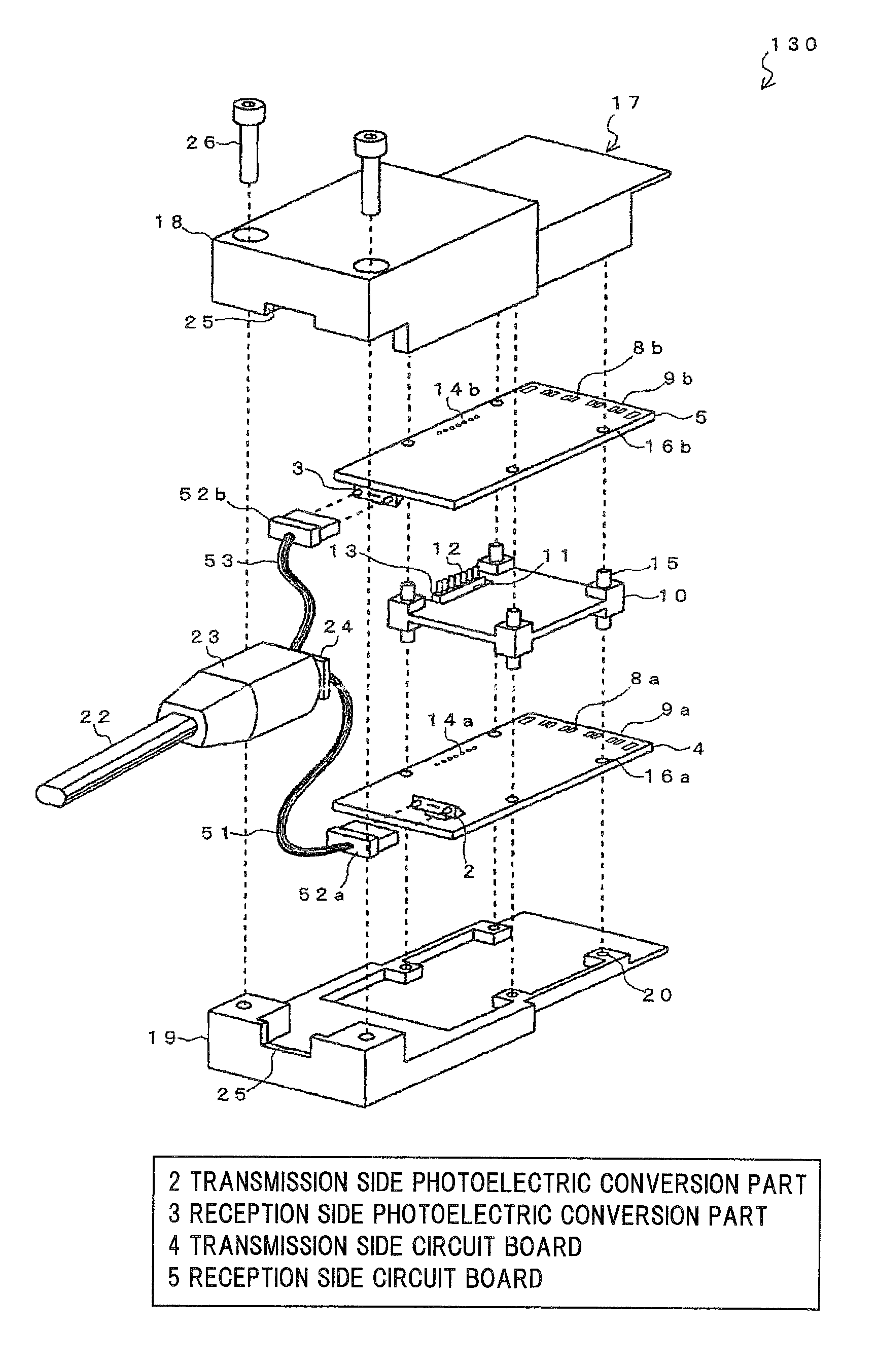
[0181]FIGS. 17 to 25 show the third embodiment of the invention. A photoelectric conversion module 130 in the third embodiment has basically the same components as the photoelectric conversion module 1. The difference from the photoelectric conversion module 1 is made such that the base member 6 is omitted and the transmission side photoelectric conversion part 2 is mounted on the transmission side circuit board 4, and that the base member 7 is omitted and the reception side photoelectric conversion part 3 is mounted on the reception side circuit board 5.
[0182]As shown in FIG. 21, the transmission side photoelectric conversion part 2 is directly mounted at one end (i.e., at end on the lower-left side in FIG. 21) of the transmission side circuit board 4. The transmission side photoelectric conversion part 2 is mounted off-center to one side (i.e., a lower-right side in FIG. 21) in the width direction of the...
PUM
 Abstract
Description
Claims
Application Information
 - R&D
- Intellectual Property
- Life Sciences
- Materials
- Tech Scout
- Unparalleled Data Quality
- Higher Quality Content
- 60% Fewer Hallucinations
Browse by: Latest US Patents, China's latest patents, Technical Efficacy Thesaurus, Application Domain, Technology Topic, Popular Technical Reports.
© 2025 PatSnap. All rights reserved.Legal|Privacy policy|Modern Slavery Act Transparency Statement|Sitemap|About US| Contact US: help@patsnap.com