Oxygen diffusion barrier comprising Ru

a diffusion barrier and oxygen technology, applied in the field of semiconductor memory devices, can solve problems such as degrading leakage curren

Active Publication Date: 2013-08-27
INTERUNIVERSITAIR MICRO ELECTRONICS CENT (IMEC VZW)
View PDF13 Cites 2 Cited by
  • Summary
  • Abstract
  • Description
  • Claims
  • Application Information

AI Technical Summary

Benefits of technology

[0015]It is an advantage of methods according to certain embodiments of the present invention that they provide reduced EOT, reduced leakage current Jg and / or reduced contact resistance between storage node and electrical contact plug, when compared to prior art methods for forming MIM capacitor structures.

Problems solved by technology

In the choice of RuO2 film formation, however, converting Ru to RuO2 by oxidation could generate some rough surface morphology which in turn degrades leakage current.

Method used


Image

  • Oxygen diffusion barrier comprising Ru
  • Oxygen diffusion barrier comprising Ru
  • Oxygen diffusion barrier comprising Ru

Examples


first embodiment

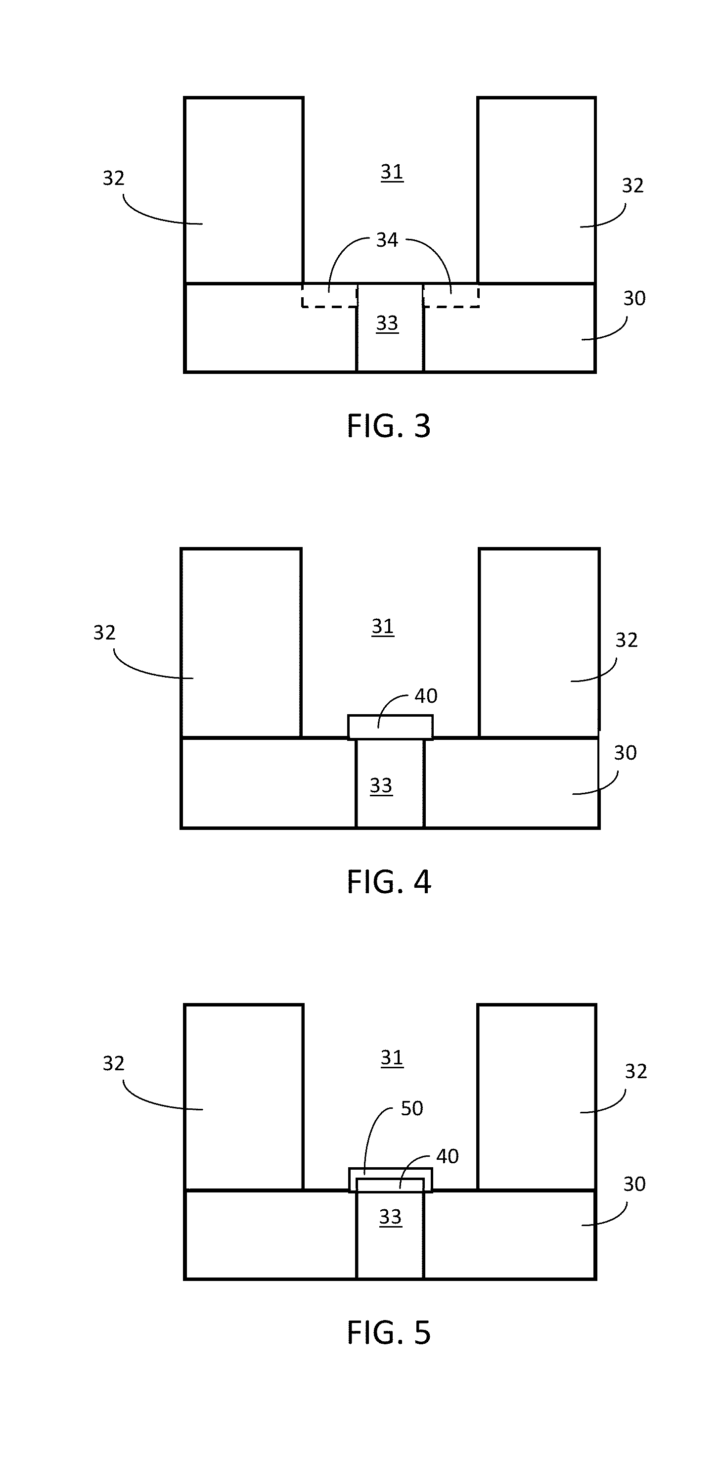
[0048]In the present invention, a method is proposed for forming an inner MIM capacitor structure. This means that a capacitor storage node container is provided, e.g. a recess or a trench in a substrate, in which a capacitor structure is provided.

[0049]FIG. 3 to FIG. 7 illustrate different steps in a method according to the first embodiment of the present invention.

[0050]In a first step 21, a base structure 30 is obtained, comprising a capacitor storage node container 31. In embodiments of the present invention, the term “base structure”30 may include any underlying material or materials that may be used, or upon which a capacitor structure in accordance with embodiments of the present invention may be formed. In particular embodiments, this base structure 30 may include a semiconductor substrate such as e.g. doped or undoped silicon, a gallium arsenide (GaAs), a gallium arsenide phosphide (GaAsP), an indium phosphide (InP), a germanium (Ge), or a silicon germanium (SiGe) substrate...

second embodiment

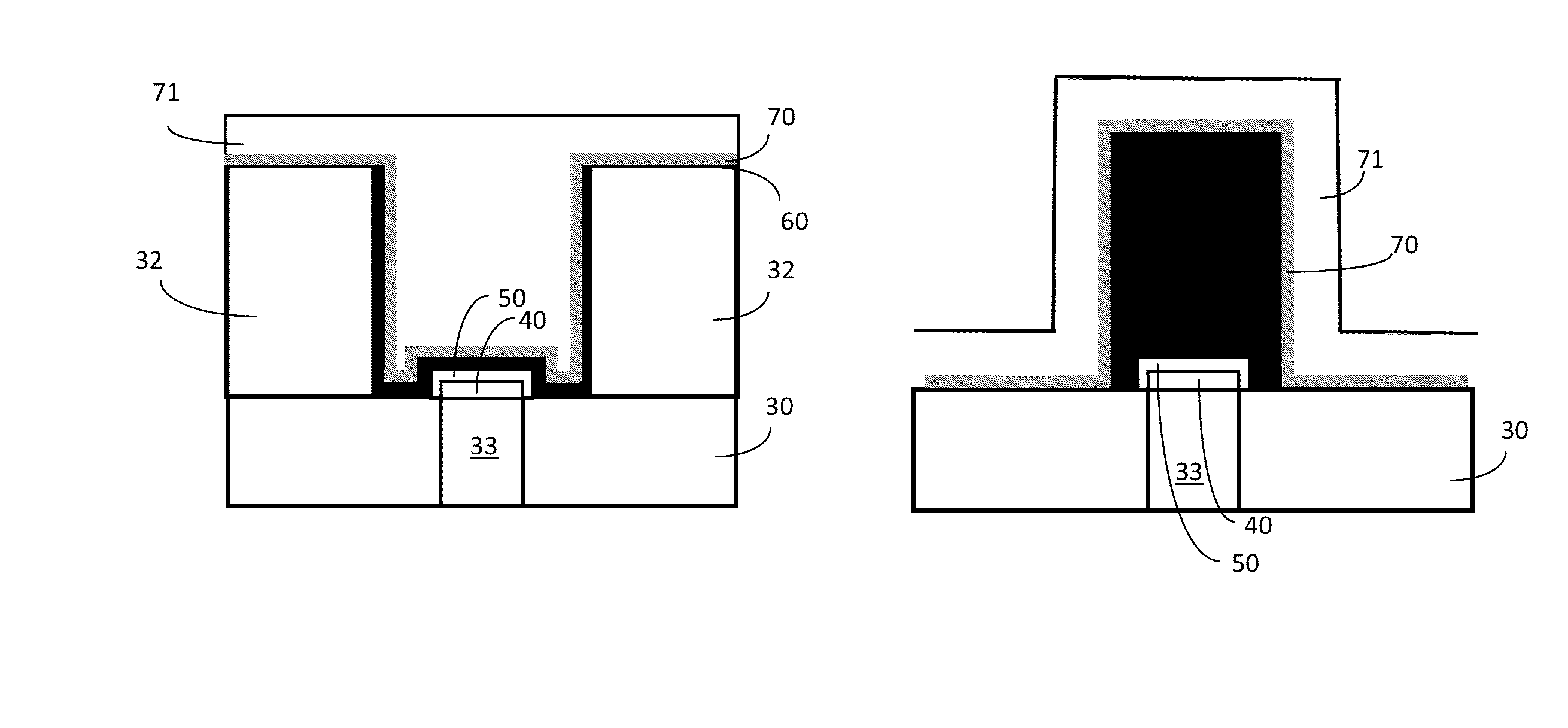
[0060]In the present invention, a method is proposed for forming an outer MIM capacitor structure. This means that a structure sticking out of a base structure is provided, over which a capacitor structure is provided.

[0061]The method according to the second embodiment of the present invention comprises a plurality of method steps, illustrated with respect to FIG. 3 to FIG. 5 and FIG. 8 and FIG. 9.

[0062]The first steps 21, 22 and 23 are as in the method according to the first embodiment of the present invention, and therefore are not recited here. Similar materials and similar methods may be used.

[0063]Once the storage node container provided with selectively grown Ru on the bottom electrode plug, based on a difference in incubation time of Ru growth on the bottom electrode plug compared to the material of the base structure, which thereafter is oxidized, in a step 24 a bottom electrode 60 is provided. In this second method embodiment, providing the bottom electrode 60 comprises sub...


PUM

PropertyMeasurementUnit
thickness EoTaaaaaaaaaa
thicknessaaaaaaaaaa
temperatureaaaaaaaaaa

Abstract

A method for forming a MIM capacitor structure includes the steps of obtaining a base structure provided with a recess, the recess exposing a conductive bottom electrode plug; selectively growing Ru on the bottom electrode plug, based on a difference in incubation time of Ru growth on the bottom electrode plug compared to the base structure material; oxidizing the selectively grown Ru; depositing a Ru-comprising bottom electrode over the oxidized Ru; forming a dielectric layer on the Ru-comprising bottom electrode; and—forming a conductive top electrode over the dielectric layer.

Description

CROSS REFERENCE TO RELATED APPLICATIONS[0001]This application claims the benefit of priority of European Patent Application no. 11186243.9, filed Oct. 21, 2011, which is hereby incorporated herein by reference in its entirety.BACKGROUND OF THE INVENTION[0002]1. Field of the Invention[0003]The present invention relates to the field of semiconductor devices, more particularly to the field of semiconductor memory devices, e.g. capacitor structures. More particularly the present invention relates to a method to selectively form Ru and / or RuO2 as an oxygen diffusion barrier in such memory devices, and to memory devices provided with such Ru-based diffusion barrier.[0004]2. Technical Background[0005]For future MIM (metal-insulator-metal) capacitor devices, Ru and RuO2 are the most interesting candidates to replace current TiN bottom and top electrodes. It has been suggested that RuO2 is more likely a candidate thanks to RuO2 reduction to Ru releasing O2 into the capacitor dielectric to he...

Claims


Application Information

Patent Timeline
Patent Type & Authority Patents(United States)
IPC IPC(8): H01L21/76
CPCC23C16/40H01L21/28562H01L28/65H01L28/75H01L21/7687C23C16/0281C23C16/045H01L21/76849H01L21/76856H01L28/90
Inventor KIM, MIN-SOOCAILLAT, CHRISTIANSWERTS, JOHAN
Owner INTERUNIVERSITAIR MICRO ELECTRONICS CENT (IMEC VZW)
Why Eureka
Try Eureka