Manufacturing method for dual work-function metal gates

a manufacturing method and metal gate technology, applied in the field of semiconductor devices having dual work function metal gates, can solve the problems of increased challenge and limitation of material selection and associated processes, abnormal threshold voltage, increased gate leakage current, etc., to reduce and increase the effective work function of the metal gate

Active Publication Date: 2018-07-26
SEMICON MFG INT (SHANGHAI) CORP +1
View PDF12 Cites 0 Cited by
  • Summary
  • Abstract
  • Description
  • Claims
  • Application Information

AI Technical Summary

Benefits of technology

[0007]In view of the above problems, the present inventor has discovered that, by performing different treatments on the surface of the gate dielectric layer that is in contact with the metal gate, the interface between the gate dielectric layer and the metal gate can be affected, so that the effective work function of the metal gate can be adjusted. Specifically, performing a nitriding treatment on the surface of the gate dielectric l

Problems solved by technology

However, this increases the challenge and limitation of the material selection and associated processes.
Further, in the case where the NMOS and PMOS devices have interconnected gates and are relatively close to an electric circuit, e.g., a static random acce

Method used


Image

  • Manufacturing method for dual work-function metal gates
  • Manufacturing method for dual work-function metal gates
  • Manufacturing method for dual work-function metal gates

Examples


first embodiment

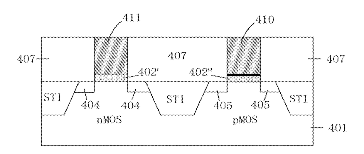
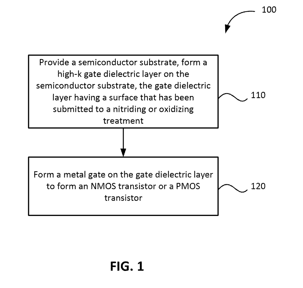
[0025]FIG. 1 is a simplified flowchart illustrating a method 100 of manufacturing a semiconductor device according to a first embodiment of the present invention. Method 100 may include, at step 110, providing a semiconductor substrate, and forming a high dielectric constant (high-k) gate dielectric layer on the semiconductor substrate. The high-k gate dielectric layer has a surface that has been subjected to a nitriding or oxidizing treatment. The semiconductor substrate is of a semiconductor material (e.g., Si, SiC, SiGe, etc.). The semiconductor substrate may include other device components, e.g., shallow trench isolation (STI), wells and / or other components formed in previous process steps.

[0026]Alternatively, prior to forming the high-k gate dielectric layer, an interface layer (e.g., SiO2) may be formed on the semiconductor substrate using a thermal growth or deposition process to improve the interface state between the high-k gate dielectric layer and the semiconductor substr...

second embodiment

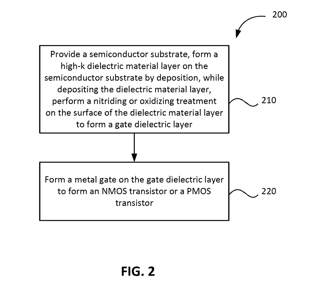
[0035]FIG. 2 is a simplified flowchart illustrating a method 200 of manufacturing a semiconductor device according to a second embodiment of the present invention. Method 200 is a specific embodiment of the first embodiment that has been described in above sections. Technical details not described herein may be referred to the corresponding description of the first embodiment.

[0036]Method 200 may include, at step 210, providing a semiconductor substrate, and forming a high dielectric constant (high-k) dielectric material layer on the semiconductor substrate using a deposition process. In the deposition process, a nitriding or oxidizing treatment is performed on the surface of the dielectric material layer so that the surface of the dielectric material layer is doped with nitrogen ions or oxygen ions. The dielectric material layer may be deposited using a variety of processes, e.g., a CVD process. The dielectric material layer may include HfO2, TiO2, or ZrO2.

[0037]Step 220 is similar...

third embodiment

[0039]FIG. 3 is a simplified flowchart illustrating a method 300 of manufacturing a semiconductor device according to a third embodiment of the present invention. Method 300 is another specific embodiment of the first embodiment that has been described in above sections. Technical details not described herein may be referred to the corresponding description of the first embodiment.

[0040]Method 300 may include, at step 310, providing a semiconductor substrate, and forming a high-k dielectric material layer on the semiconductor substrate using a deposition process. The dielectric material layer may be deposited using a variety of processes, such as a CVD process. The dielectric material layer may include HfO2, TiO2, or ZrO2.

[0041]At step 312, a nitriding or oxidizing treatment is performed on the surface of the dielectric material layer to form a gate dielectric layer having at least a nitrided surface or an oxidized surface.

[0042]In one embodiment, the nitriding treatment may include...


PUM


Abstract

A method for manufacturing a semiconductor device includes providing a semiconductor substrate, forming a high dielectric constant (high-k) gate dielectric layer on the semiconductor substrate, the high-k gate dielectric layer including a nitrided surface that has been subjected to a nitriding treatment or an oxidized surface that has been subjected to an oxidizing treatment, forming a metal gate on the nitrided surface of the high-k gate dielectric layer to form an NMOS transistor, or forming a metal gate on the oxidized surface of the high-k gate dielectric layer to form a PMOS transistor.

Description

CROSS-REFERENCES TO RELATED APPLICATIONS[0001]The present application claims priority to Chinese patent application No. 201710045041.6, filed with the State Intellectual Property Office of People's Republic of China on Jan. 22, 2017, the content of which is incorporated herein by reference in its entirety.FIELD OF THE INVENTION[0002]The present disclosure relates to semiconductor technology, and more particularly to a semiconductor device having dual work-function metal gates and manufacturing method thereof.BACKGROUND OF THE INVENTION[0003]With the development of integrated circuit technology, the feature sizes of semiconductor devices are getting smaller and smaller. Current complementary metal-oxide semiconductor (CMOS) devices use a high dielectric-constant (high-k) material as the gate dielectric layer and a metal as the gate electrode (HKMG).[0004]For NMOS and PMOS devices, the expected work function of the metal gate is quite different, which is about 4.1 eV to about 4.4 eV a...

Claims


Application Information

Patent Timeline
IPC IPC(8): H01L21/8238H01L27/092H01L29/51H01L29/49H01L29/66H01L21/28H01L21/02
CPCH01L21/823857H01L27/092H01L29/517H01L29/4966H01L29/66545H01L21/823842H01L21/28202H01L21/28211H01L21/02181H01L21/02186H01L21/28088H01L21/28185H01L29/66477H01L29/78
Inventor ZHANG, QINGCHUN
Owner SEMICON MFG INT (SHANGHAI) CORP
Why Eureka
Try Eureka