Method and gate structure for threshold voltage modulation in transistors

a threshold voltage and transistor technology, applied in the field of semiconductor devices, can solve the problems of fermi level pinning effect, difficult to form metal gate electrodes with n-type work functions and p-type work functions, and achieve the effect of increasing preventing the increase of the effective work function of the gate stack

Active Publication Date: 2015-05-07
SK HYNIX INC
View PDF15 Cites 17 Cited by
  • Summary
  • Abstract
  • Description
  • Claims
  • Application Information

AI Technical Summary

Benefits of technology

[0012]Moreover, according to the embodiments, since an oxidation suppressing layer is formed on the N type work function gate electrode, it is possible to substantially prevent the effective work function of a gate stack from being increased.
[0013]Further, according to the embodiments, since an oxide is formed on the P type work function gate electrode, it is possible to increase the effective work function of a gate stack.

Problems solved by technology

However, the use of the high-k material creates a concern of a Fermi level pinning effect.
However, when fabricating a CMOS device, it is difficult to form metal gate electrodes with an N-type work function and a P-type work function that require threshold voltages (Vt) appropriate for respective transistors.

Method used


Image

  • Method and gate structure for threshold voltage modulation in transistors
  • Method and gate structure for threshold voltage modulation in transistors
  • Method and gate structure for threshold voltage modulation in transistors

Examples


first embodiment

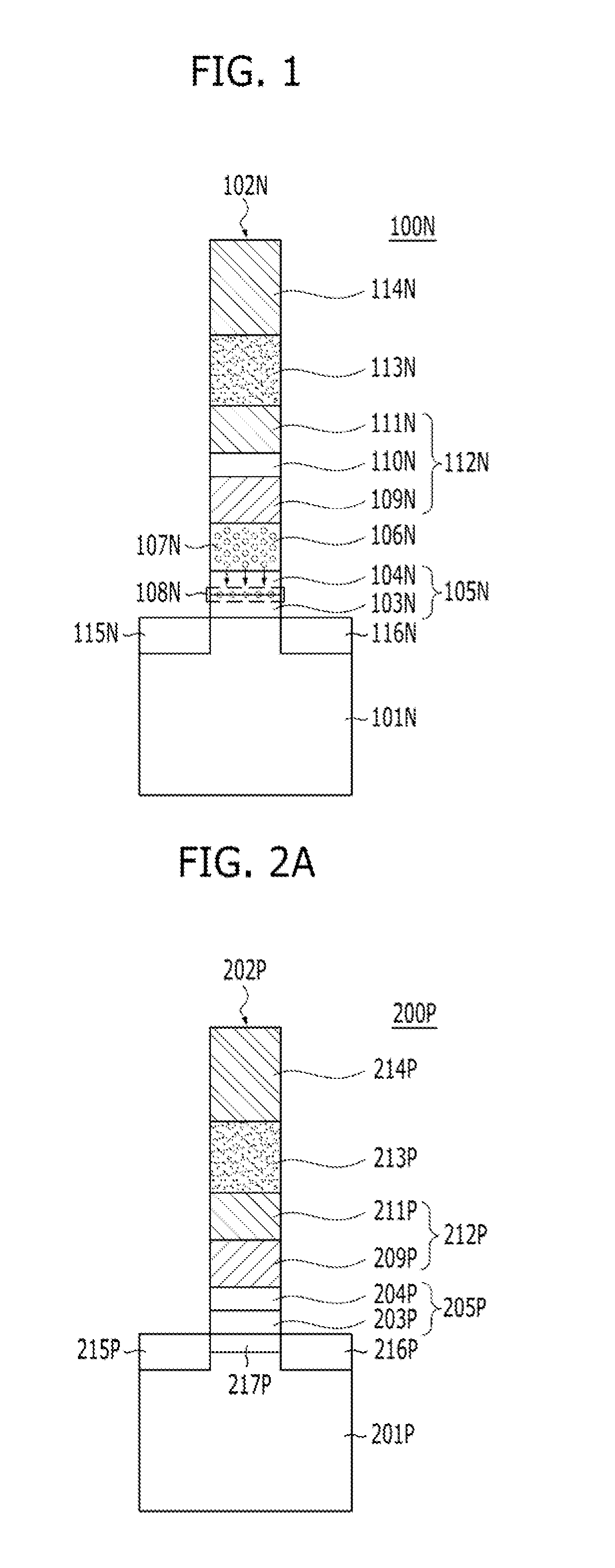
[0040]In the first embodiment, a flat band voltage is decreased due to a dipole effect by the dipole-interface 108N. Further, a work function is decreased by the oxidation suppressing layer 110N.

[0041]Accordingly, the threshold voltage of the transistor 100N may be shifted in a desired direction.

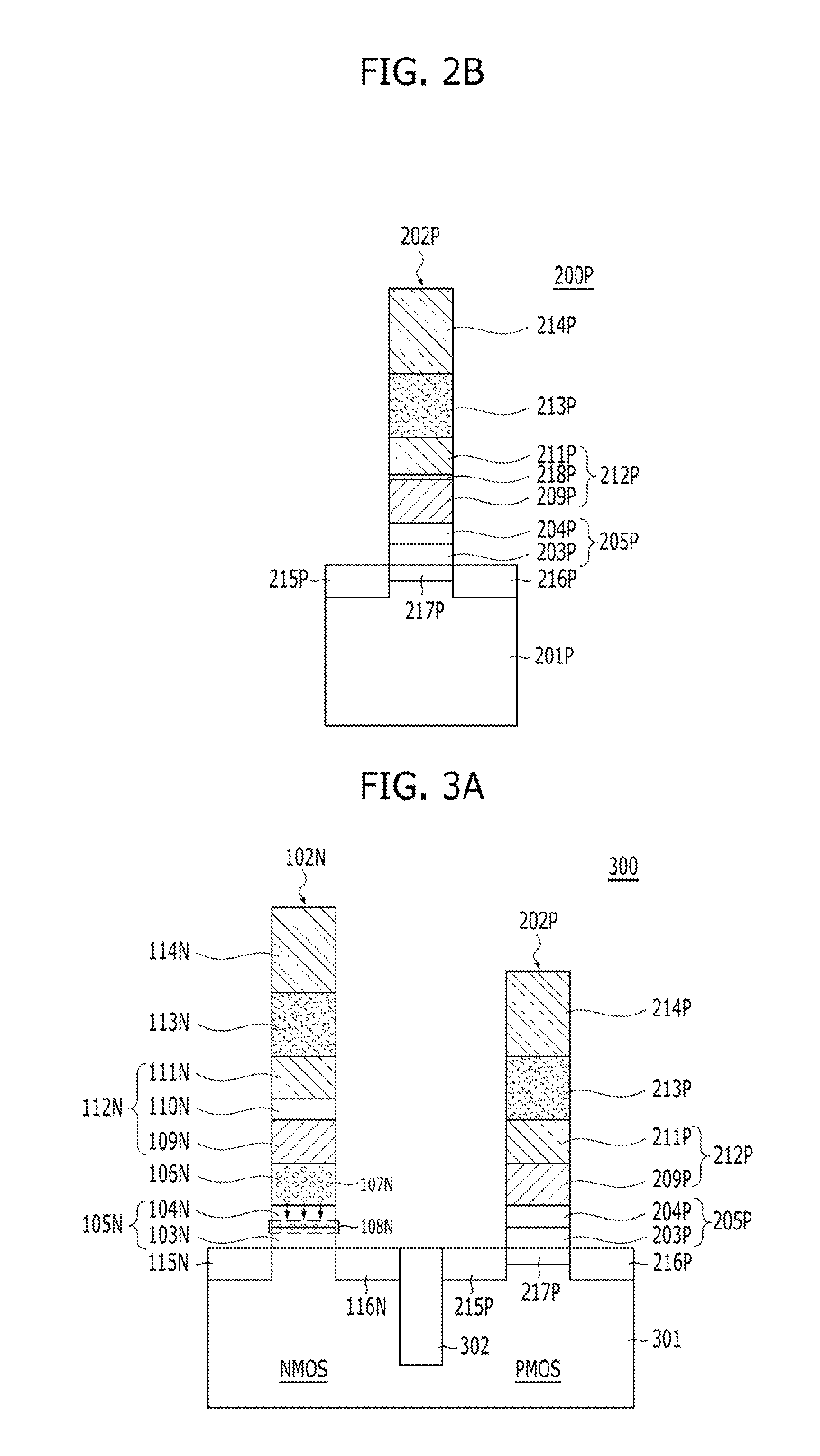
[0042]FIG. 2A is a view illustrating a transistor in accordance with a second embodiment. FIG. 2B is a view illustrating a transistor in accordance with a variation of the second embodiment.

[0043]Referring to FIGS. 2A and 2B, a transistor 200P may include a gate stack 202P, a source region 215P and a drain region 216P. The transistor 200P may include a P-channel transistor. The transistor 200P may include a PMOSFET.

[0044]The gate stack 202P is formed on a substrate 201P. The gate stack 202P may include a gate dielectric layer 205P, and a gate electrode 212P. The gate dielectric layer 205P may include an interface layer 203P and a high-k dielectric layer 204P. The gate electrode 212P may incl...

second embodiment

[0053]In the present second embodiment, the threshold voltage of the transistor 200P is modulated due to a valence band offset by the germanium-containing channel region 217P. Furthermore, the threshold voltage of the transistor 200P is modulated by the surface oxidation of the first work function layer 209P and the thick thickness of the first work function layer 209P and the second work function layer 211P.

[0054]As a result, the threshold voltage of the transistor 200P may be shifted in a desired direction. Moreover, since the germanium-containing channel region 217P may include the SiGe / Si epitaxial layer, threshold voltage modulation becomes easier.

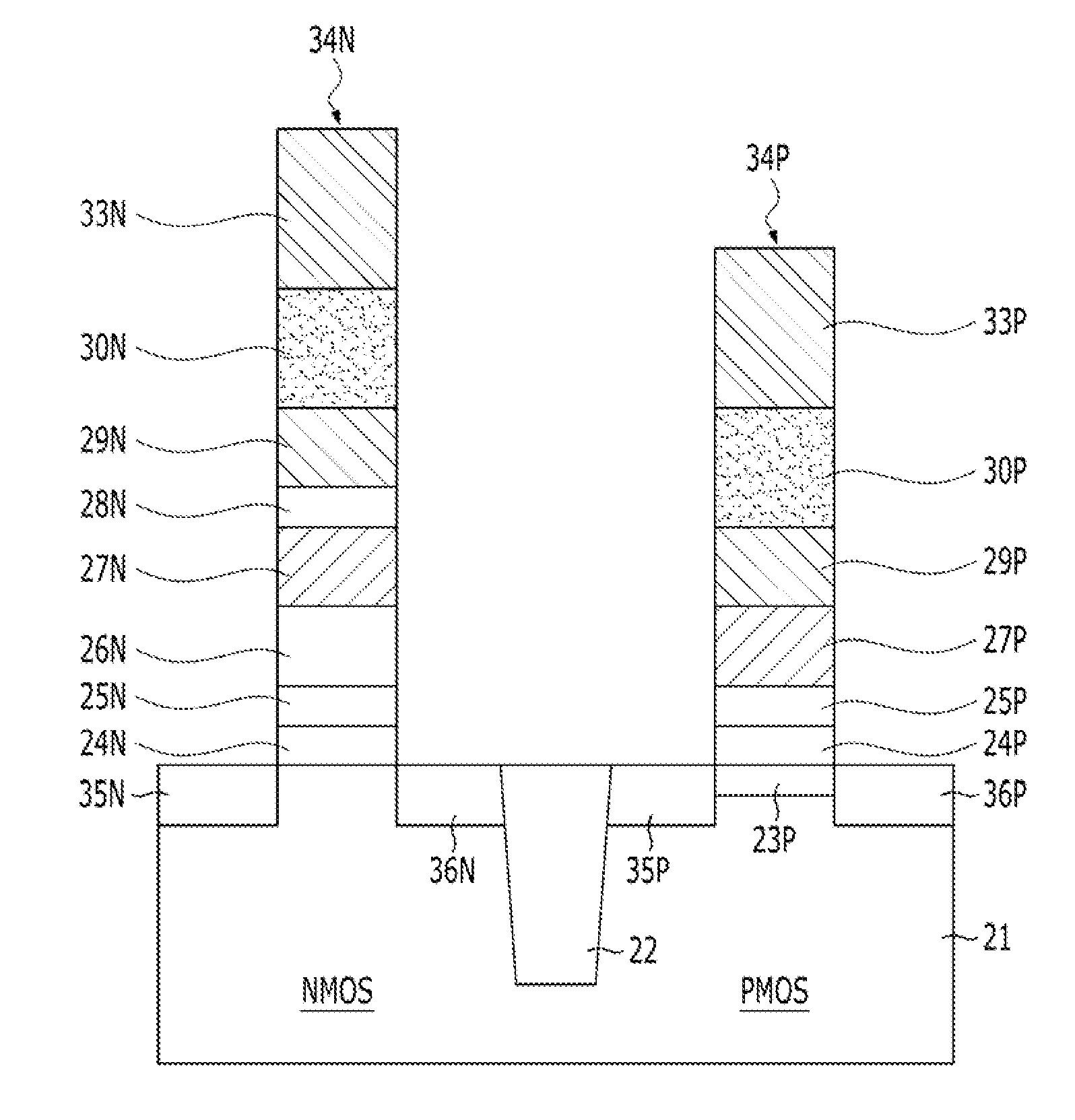
[0055]FIG. 3A is a view illustrating an exemplary CMOS device to which the first exemplary implementation and the second exemplary implementation are applied. FIG. 3A shows a CMOSFET in which the N-channel transistor of FIG. 1 and the P-channel transistor of FIG. 2A are integrated. FIG. 3B is a view illustrating an exemplary CMOS devi...


PUM


Abstract

A method of fabricating a semiconductor device. A substrate (PMOS/NMOS regions) is prepared. A high-k dielectric layer is formed over the substrate. A threshold voltage modulation layer is formed over the dielectric layer of the NMOS region. A first work function layer is formed over the threshold voltage modulation layer and the dielectric layer of the PMOS region. An oxidation suppressing layer is formed over the first work function layer of the NMOS region. A second work function layer is formed over the oxidation suppressing layer and the first work function layer of the PMOS region. A first gate stack including the dielectric layer, the first work function layer and the second work function layer is formed over the PMOS region. A second gate stack including the dielectric layer, the threshold voltage modulation layer, the first work function layer and the oxidation suppressing layer is formed over NMOS region.

Description

CROSS-REFERENCE TO RELATED APPLICATIONS[0001]The present application claims priority of Korean Patent. Application No. 10-2013-0132918, filed on Nov. 4, 2013, which is incorporated herein by reference in its entirety.BACKGROUND[0002]1. Field[0003]Exemplary embodiments of the present invention relate to a semiconductor device, and more particularly, to a method and a gate structure for threshold voltage modulation in transistors.[0004]2. Description of the Related Art[0005]If a transistor is scaled down to improve the performance thereof, gate leakage may increase as a thickness of a gate dielectric layer is reduced. In order to cope with this concern, the material of a gate dielectric layer may be replaced with a high-k material having a dielectric constant that is larger than the dielectric constant of SiO2. The high-k material may include a metal oxide containing hafnium, zirconium, or the like. However, the use of the high-k material creates a concern of a Fermi level pinning eff...

Claims


Application Information

Patent Timeline
Patent Type & Authority Applications(United States)
IPC IPC(8): H01L27/092H01L29/51H01L21/8238
CPCH01L27/0922H01L29/512H01L21/823857H01L21/823878H01L21/28202H01L29/1054H01L29/4966H01L29/513H01L29/517H01L29/518H01L29/78H01L21/18
Inventor JI, YUN-HYUCKJOO, MOON-SIGJANG, SE-AUGLEE, SEUNG-MIKIM, HYUNG-CHUL
Owner SK HYNIX INC
Why Eureka
Try Eureka