Solid-state imaging apparatus

a solid-state imaging and apparatus technology, applied in the direction of television systems, radiation controlled devices, color signal processing circuits, etc., can solve the problems of difficult suppression of signal variation, “false signal”, and inability to easily reduce the power source voltage in view of the performance of the solid-state imaging apparatus, etc., to reduce layout dimensions, reduce pixel sizes, and reduce pixel sizes

Inactive Publication Date: 2013-08-27
CANON KK
View PDF61 Cites 11 Cited by
  • Summary
  • Abstract
  • Description
  • Claims
  • Application Information

AI Technical Summary

Benefits of technology

[0005]As pixel sizes have been reduced according to a recent multipixel tendency, it is required to also reduce layout dimensions of signal processing circuits. A signal processing circuit disposed in a column direction of pixels arranged in a two-dimensional matrix form is narrowly disposed in the vertical direction of the matrix. As the pixel sizes are reduced, it is required to lay out the circuit in a narrower width. In Japanese Patent Application Laid-Open No. 2005-217158, in order to reduce the layout width of the signal processing circuit, it is required to reduce dimensions of transistors or change directions of channels of the transistors. The dimensions of transistors are restricted by power source voltage of the circuit, resolution of a stepper used in a manufacturing process, and alignment accuracy. In particular, the power source voltage cannot easily be reduced in view of performance of the solid-state imaging apparatus. This is because the signal processing circuit of the solid-state imaging apparatus includes analog circuit and reduction in power source voltage directly causes reduction in dynamic range. The narrower the width of a wiring, the greater the resistance of the wiring becomes. Accordingly, it becomes difficult to suppress variation in signal when voltage changes. Thus, there is a case of causing a problem in that signals of a certain signal processing circuit cause a “false signal” in another signal processing circuit.
[0006]It is an object of the present invention to provide a solid-state imaging apparatus capable of suppressing a false signal.

Problems solved by technology

In particular, the power source voltage cannot easily be reduced in view of performance of the solid-state imaging apparatus.
Accordingly, it becomes difficult to suppress variation in signal when voltage changes.
Thus, there is a case of causing a problem in that signals of a certain signal processing circuit cause a “false signal” in another signal processing circuit.

Method used


Image

  • Solid-state imaging apparatus
  • Solid-state imaging apparatus
  • Solid-state imaging apparatus

Examples


first embodiment

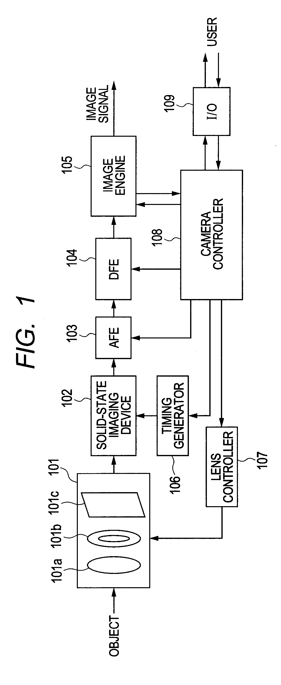
[0018]FIG. 1 is a block diagram illustrating an example of a configuration of a solid-state imaging apparatus according to a first embodiment of the present invention. The solid-state imaging apparatus may be, for example, one of a digital single lens reflex camera, a compact digital camera, a video camera, a cellular phone digital camera and a broadcasting digital camera. The solid-state imaging apparatus includes an optical system 101, a solid-state imaging device 102, an AFE 103, a DFE 104, an image engine 105, a timing generator 106, a lens controller 107, a camera controller 108 and an interface 109. The AFE 103 is an analog frontend. The DFE is a digital frontend. The optical system 101 includes a lens 101a forming an image of incident light from an object on an imaging surface of an solid-state imaging device 102, a diaphragm 101b controlling the amount of incident light passing through the lens 101a and a shutter 101c, and the shutter 101c controlling the time of light incid...

second embodiment

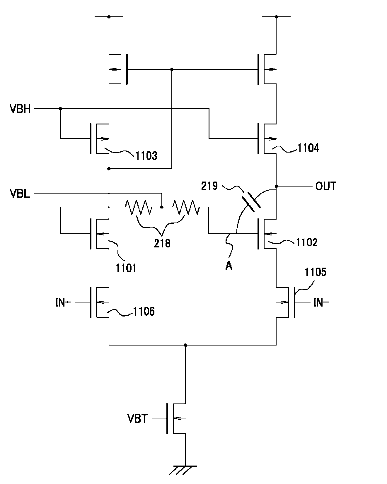
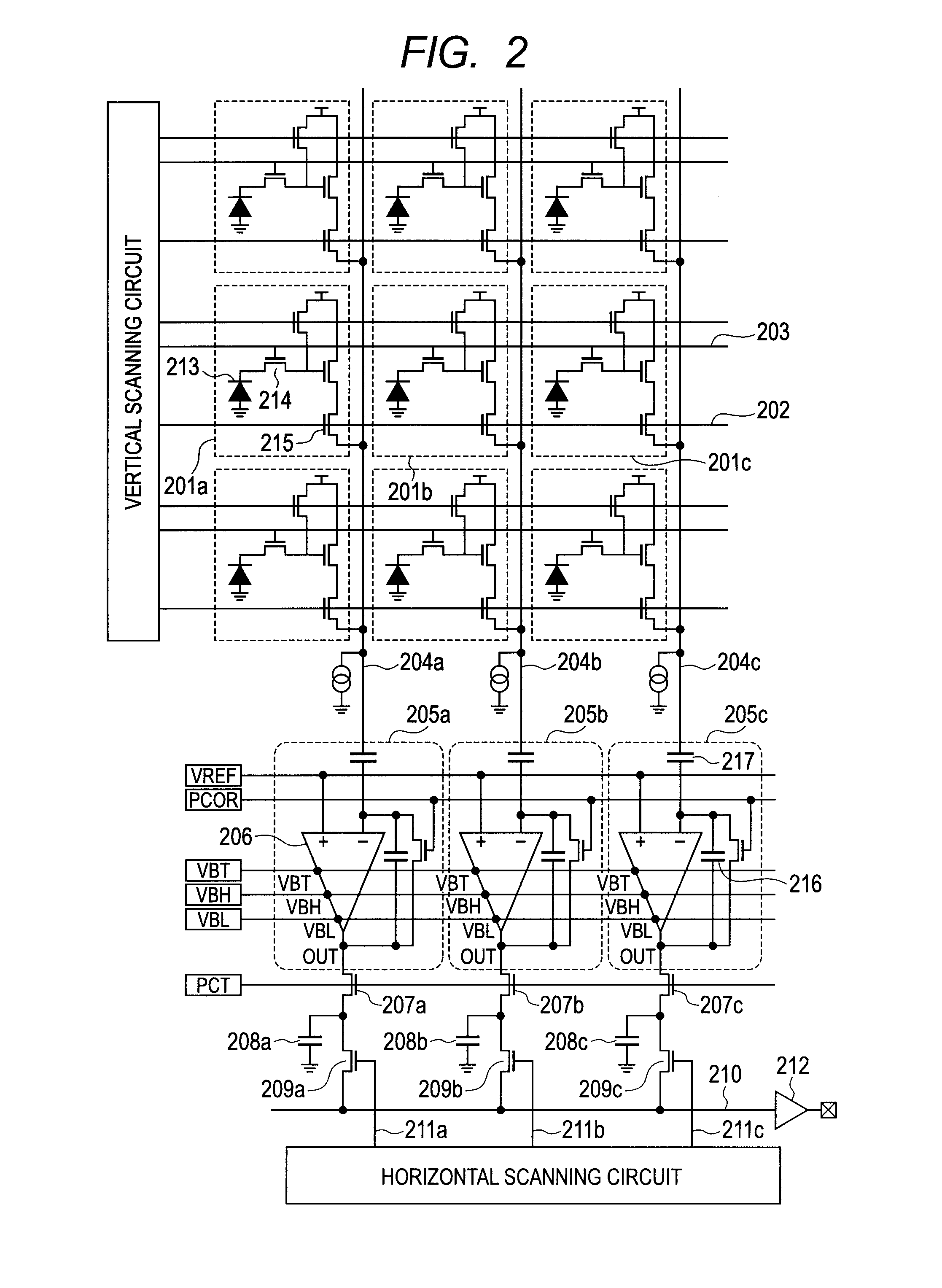
[0033]FIG. 7 is a pattern layout diagram of amplifiers 206 of signal processing circuits 205a to 205c according to a second embodiment of the present invention. Transistors 1101, 1102, 1105 and 1106 include gate electrodes 1101G, 1102G, 1105G and 1106G having a comb shape. Thus, the transistors 1101, 1102, 1105 and 1106 are configured by a parallel connection circuit of transistors. Accordingly, the channel width is widened and a high gm is attained, thereby achieving high open loop gain. In this case, the distance D14 between the gate electrode 1101G of the transistor 1101 and the gate electrode 1102G of the transistor 1102 configuring the cascode circuit is further increased, thereby allowing the advantageous effects of this embodiment to be more significant. As with the first embodiment, even with the silicide gate material, the advantageous effect of this embodiment can be attained.

[0034]The first and second embodiments reduce the resistances of the wirings 402 to 406 connected ...


PUM


Abstract

A solid-state imaging apparatus is provided that including a plurality of amplifiers each one amplifying a signal from each one of a plurality of pixels. The amplifier including first and second field effect transistors, gate electrodes of which are connected to the same voltage node (VBL); and a first wiring connected between the voltage node and the gate electrodes of the first and second field effect transistors. The first and second field effect transistors are arranged in a direction perpendicular to a direction in which the plurality of amplifiers is arranged. Material of the first wiring has a resistivity smaller than that of the gate electrodes of the first and second field effect transistors.

Description

BACKGROUND OF THE INVENTION[0001]1. Field of the Invention[0002]The present invention relates to a solid-state imaging apparatus.[0003]2. Description of the Related Art[0004]An active solid-state imaging apparatus, such as a CMOS image sensor is provided with pixels including photoelectric conversion devices, and signal processing circuits processing electric signals of the pixels. Japanese Patent Application Laid-Open No. 2005-217158 discloses a solid-state imaging apparatus including a signal processing circuit. This document discloses the signal processing circuit that receives pixel signals from pixel columns via a signal output line and amplifies or processes the signals. A method is effective that applies high gain to the signal processing circuit in order to compensate reduction in sensitivity owing to reduction of pixel areas. Thus, an amplifier including a cascode circuit is used.SUMMARY OF THE INVENTION[0005]As pixel sizes have been reduced according to a recent multipixel...

Claims


Application Information

Patent Timeline
Patent Type & Authority Patents(United States)
IPC IPC(8): H04N9/64H04N3/14H01L27/148
CPCH03F3/45188H04N5/357H04N5/378H03F2203/45646H04N25/60H04N25/75
Inventor OGURA, MASANORIYAMASHITA, YUICHIROKOIZUMI, TORU
Owner CANON KK
Why Eureka
Try Eureka