Semiconductor integrated circuit, method of manufacturing semiconductor integrated circuit, charge pump circuit, layout designing apparatus, and layout designing program

a semiconductor integrated circuit and integrated circuit technology, applied in the field of semiconductor integrated circuits, can solve the problems of complex layout of transistors to transistors, increased layout area, and inability to easily change layouts, etc., and achieve the effect of increasing display area, low degree of design freedom, and increasing layout width

Active Publication Date: 2007-01-04
NEC LCD TECH CORP
View PDF10 Cites 5 Cited by
  • Summary
  • Abstract
  • Description
  • Claims
  • Application Information

AI Technical Summary

Benefits of technology

[0035] According to a twenty-second aspect of the present invention, in the semiconductor integrated circuit according to the nineteenth aspect, at least one of the source and drain electrodes of the transistors to be connected to an external terminal is extended for connection to the external terminal. This arrangement ensures that a semiconductor integrated circuit can be provided which is capable of being connected to external input / output terminals without increasing the layout width even in a case where the external input / output terminals are concentrated on one side so that the degree of design freedom is low.
[0036] According to a twenty-third aspect of the present invention, there is provided a semiconductor integrated circuit according to the sixteenth aspect, the transistors are thin-film transistors formed on a glass substrate or an insulation substrate other than a semiconductor substrate. This arrangement makes it possible to provide a display or a sensor in which a peripheral circuit is mounted in a small-width layout on a display substrate or a sensor substrate with integrated thin-film transistors, and which has an increased display area or an increased sensing region.
[0037] According to a twenty-fourth aspect of the present invention, there is provided a method of manufacturing the semiconductor integrated circuit according to the twenty-third aspect, including advancing crystallization in the gate width direction in a step of crystallizing an amorphous semiconductor layer into a polycrystalline semiconductor. According to this method, the transistors can be crystallized simultaneously with each other and performance variations between the transistors are thereby reduced.

Problems solved by technology

This area is always smaller than the area shown in FIG. 33 if W>0. In this layout, however, a change in layout cannot be made easily because the optimum parallel gate placement varies from transistor to transistor if the complexity of the circuit is increased.
In such circuit layouts, however, the layout area is increased or the transistor-to-transistor layout is complicated and a change in layout cannot be easily made.

Method used


Image

  • Semiconductor integrated circuit, method of manufacturing semiconductor integrated circuit, charge pump circuit, layout designing apparatus, and layout designing program
  • Semiconductor integrated circuit, method of manufacturing semiconductor integrated circuit, charge pump circuit, layout designing apparatus, and layout designing program
  • Semiconductor integrated circuit, method of manufacturing semiconductor integrated circuit, charge pump circuit, layout designing apparatus, and layout designing program

Examples


first embodiment

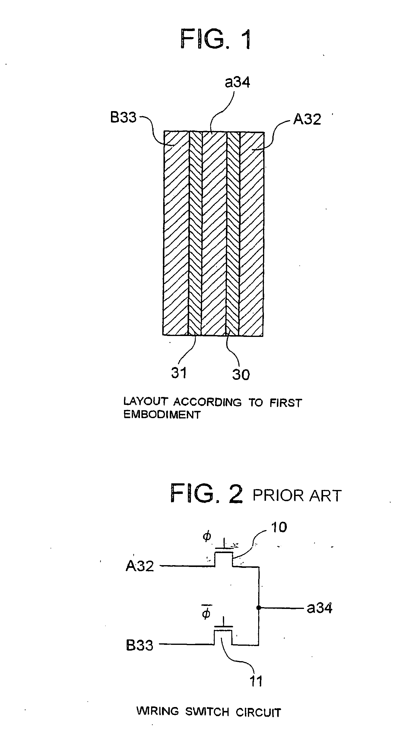
[0072] Embodiments of the present invention will be described in detail with reference to the accompanying drawings. FIG. 1 shows a layout which represents the present invention. This layout corresponds to the circuit shown in FIG. 2 as a circuit for switching the connection of a power supply line a34 between power supply lines A32 and B33. The power supply lines A32, a34, and B33 are placed in the above-mentioned order, and transistors 10 and 11 are placed in the gaps between the power supply lines A32, a34, and B33. In the layout shown in FIG. 1, each transistor has one gate electrode. The gate electrode of the transistor 10 is indicated by 30 and the gate electrode of the transistor 11 is indicated by 31. The gate electrodes 30 and 31 are placed on the opposite sides of the power supply line a34, and each gate electrode is formed by a gate layer. The power supply lines are each formed by a first metal layer and are electrically connected to active regions in the bodies of the tra...

second embodiment

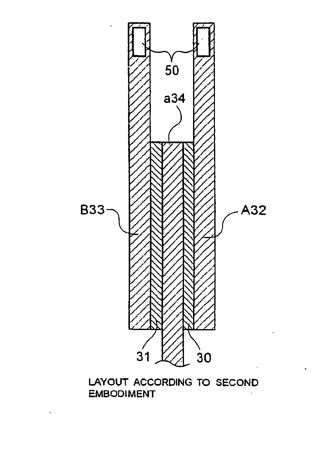
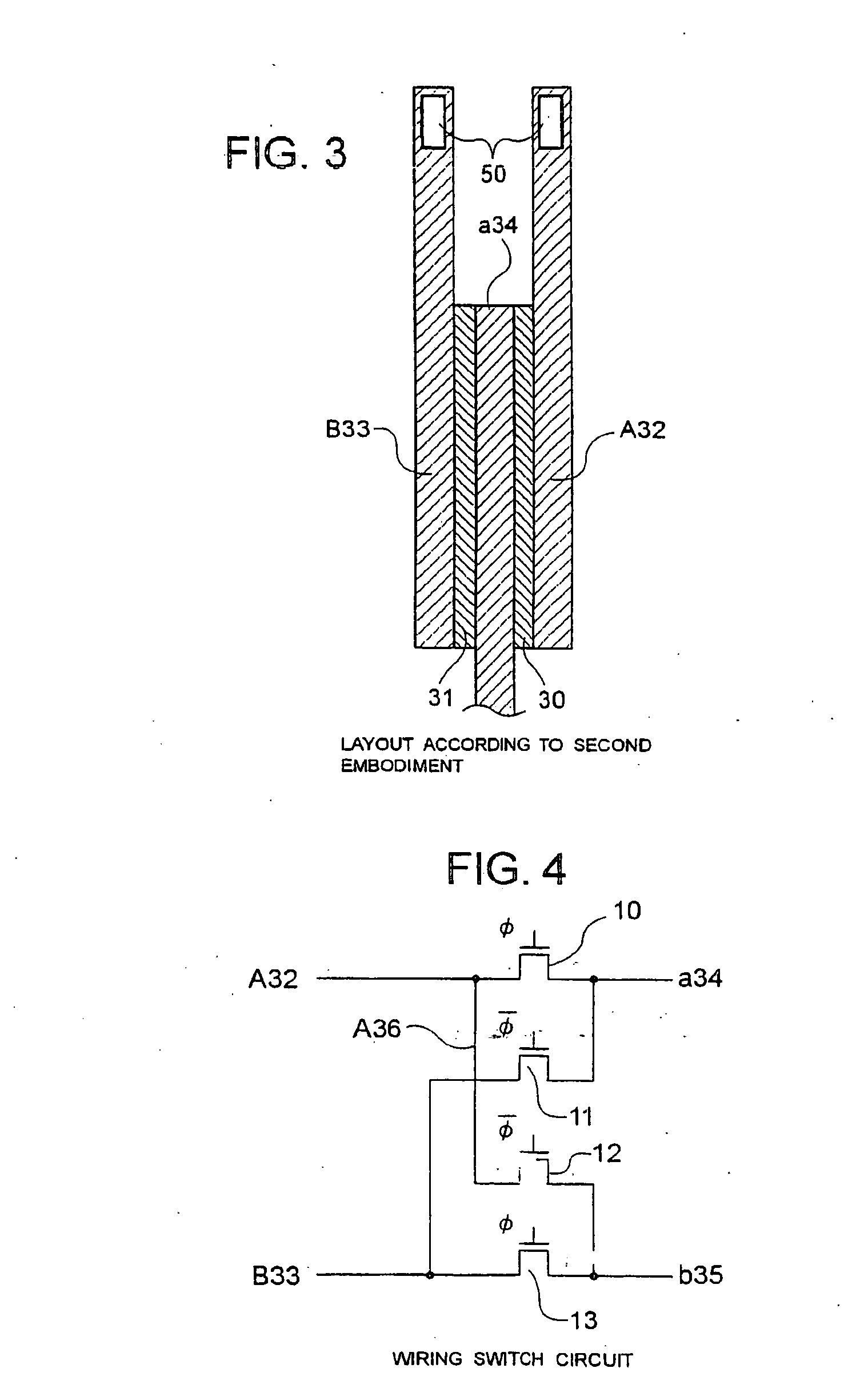
[0074]FIG. 3 is a diagram showing a layout which represents the present invention. In this embodiment, a function for connection to external terminals concentrated on one side is added to the layout shown in FIG. 1. To externally apply potentials to the power supply lines A32 and B33, the power supply lines are extended upward as viewed in the figure in wiring using the first metal layer, thereby enabling connection through external connection terminals 50. The power supply line a34 is extended downward as viewed in the figure as wiring for connection to another internal circuit. This layout is characterized by avoiding an increase in width of the circuit layout even though wiring extensions are made.

third embodiment

[0075]FIG. 5 is a diagram showing a layout which represents the present invention. This layout corresponds to a wiring switching circuit shown in FIG. 4. In this circuit, connections are exclusively made between power supply lines A32 and B33 and power supply lines a34 and b35. This circuit operates as described below. When the gate signal φ is high level, the transistors 10 and 13 are in the on state, the power supply lines A32 and a34 are connected to each other, and the power supply lines B33 and the power supply line b35 are also connected to each other. When the gate signal φ is low level, the transistors 11 and 12 are in the on state and reverse connections are established, that is, the power supply lines A32 and b35 are connected to each other, and the power supply lines B33 and the power supply line a34 are connected to each other namely resulting in reverse connection. For example, this circuit is used as a polarity reversing circuit. The power supply lines a34 and b35 are ...


PUM


Abstract

A layout capable of placing a circuit constituted by a plurality of transistors in a small-with region is automatically formed. A search section inputs data on a circuit and makes a search for a set of routes formed so that passage through any one of the transistors occurs only one time and so that the combination of routes in one set can cover the entire circuit network. An extraction section extracts a set of routes having the smallest number of routes in sets of route found by searching. A width determination section determines the layout width from the widths of source and drain electrodes of each transistor, the width of the region between the source and drain electrodes, the width of the region between some of the adjacent pairs of the transistors not combined into a common electrode, the number of transistors, and the smallest number of routes. A layout determination section forms information on a layout in which all the source, drain and gate electrodes of the transistor included in the circuit are placed in a small-width region having the determined width.

Description

BACKGROUND OF THE INVENTION [0001] 1. Field of the Invention [0002] The present invention relates to a semiconductor integrated circuit having transistors formed on a semiconductor substrate, an insulation substrate or a glass substrate and, more particularly, to a semiconductor integrated circuit capable of being laid out in a small-width region and a circuit layout designing method enabling such layout. [0003] 2. Description of the Related Art [0004] For display devices and sensors, a method has generally been used in which peripheral circuits for driving a group of transistors (active matrix) for controlling display elements or sensor elements are mounted around a display region or a sensing region or formed on the same substrate as that for the active matrix (see, for example, patent documents 1 and 2 shown below. To increase the display region or the sensing region, the peripheral circuit is placed in straight narrow regions around the display region or the sensing region. A sm...

Claims


Application Information

Patent Timeline
Patent Type & Authority Applications(United States)
IPC IPC(8): H01L27/10G06F17/50H01L21/77H01L21/82H01L21/822H01L21/84H01L23/528H01L27/02H01L27/04H01L27/12
CPCG06F17/5068G06F17/5077H01L23/5286H01L27/0207H01L2924/0002H01L27/1214H01L2924/00G06F30/39G06F30/394
Inventor NONAKA, YOSHIHIRO
Owner NEC LCD TECH CORP
Why Eureka
Try Eureka