Thin film transistor, method for manufacturing same, and liquid crystal display device using same

a thin film transistor and liquid crystal display technology, applied in semiconductor devices, radio frequency controlled devices, instruments, etc., can solve the problems of increasing the layout area of the driver circuit section, increasing the reliability of the liquid crystal projector, and increasing the deterioration of the tft characteristics. , to achieve the effect of preventing the increase of the layout area and lowering the reliability

Inactive Publication Date: 2005-05-03
SHARP KK
View PDF9 Cites 19 Cited by
  • Summary
  • Abstract
  • Description
  • Claims
  • Application Information

AI Technical Summary

Benefits of technology

[0014]The object of the present invention is to provide a thin film transistor (TFT) capable of preventing the increase of a layout area without lowering reliability; a method of manufacturing the same; and a liquid crystal device using the same.
[0016]With this arrangement, by dividing the channel region of the thin film transistor (TFT) into a plural number, drain current Id that flows the respective channel regions (divided channel regions) can be reduced. This consequently reduces the self-heating at the respective channel regions, thereby reducing the variation in threshold voltage which is the deterioration of the TFT characteristics. Further, the source regions (divided source regions) are connected with one another, the drain regions (divided drain regions) are connected with one another, and a pair of each of the source regions and each of the drain regions sandwiches each of the channel regions. Therefore, the channel regions are connected in parallel with one another, so that the total amount of the drain current Id that flows each of the channel regions can be the same as the drain current Id of an undivided single-unit TFT.
[0019]Namely, the TFT is so arranged that the spacing between the channel regions (channel spacing) is smaller than the channel width of the channel region, with satisfying the conditions such that the spacing between the channel regions (channel spacing) is not less than 3 μm and the channel width of the channel region is not more than 50 μm. With this arrangement, without lowering the reliability of the TFT, it is possible to reduce the TFT layout width in comparison with the TFT layout width of the conventional arrangement in which the spacing between the channel regions is set to be the same as the channel width of the channel region (channel divided width), thereby reducing the increase of the TFT layout area due to the channel division.
[0021]With this arrangement, the TFT having the above-described features is used in the liquid crystal display device. Therefore, it is possible to provide a liquid crystal display device capable of obtaining the reliability as well as capable of minimizing the increase of an area of the liquid crystal display device without narrowing the pixel pitch and without lowering the open area ratio.
[0023]With this method, without lowering the reliability of the TFT of the conventional arrangement, it is possible to provide the TFT of the present invention capable of minimizing the increase of the TFT layout width due to the channel division, namely the increase from the layout width of the undivided single-unit TFT, thereby minimizing the increase of the TFT layout area due to the division.

Problems solved by technology

Operation of the TFT, however, generates a variation in threshold voltage and a resultant lowering of driving current, thereby causing a serious problem in the reliability of the liquid crystal projector.
This makes it difficult for the TFT to dissipate the heat generated by the self-heating, resulting in that the deterioration of the TFT characteristics becomes more serious than ever.
This results in the driver circuit section having a very large layout area.
As a result, in the above-described conventional arrangement, it is quite difficult to obtain both the TFT reliability and the retained open area ratio without increasing the size of the liquid crystal panel.

Method used


Image

  • Thin film transistor, method for manufacturing same, and liquid crystal display device using same
  • Thin film transistor, method for manufacturing same, and liquid crystal display device using same
  • Thin film transistor, method for manufacturing same, and liquid crystal display device using same

Examples


example 1

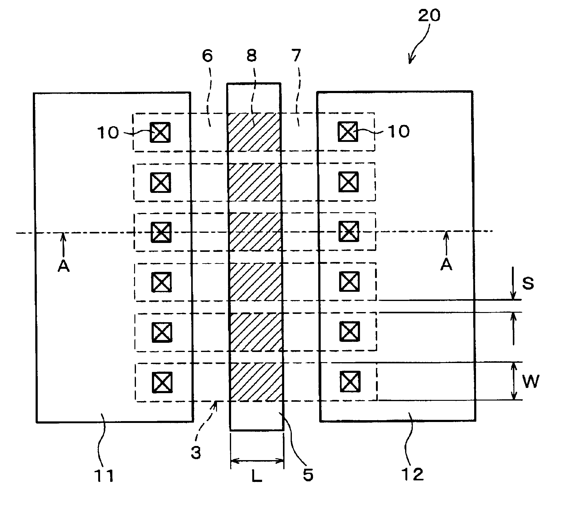
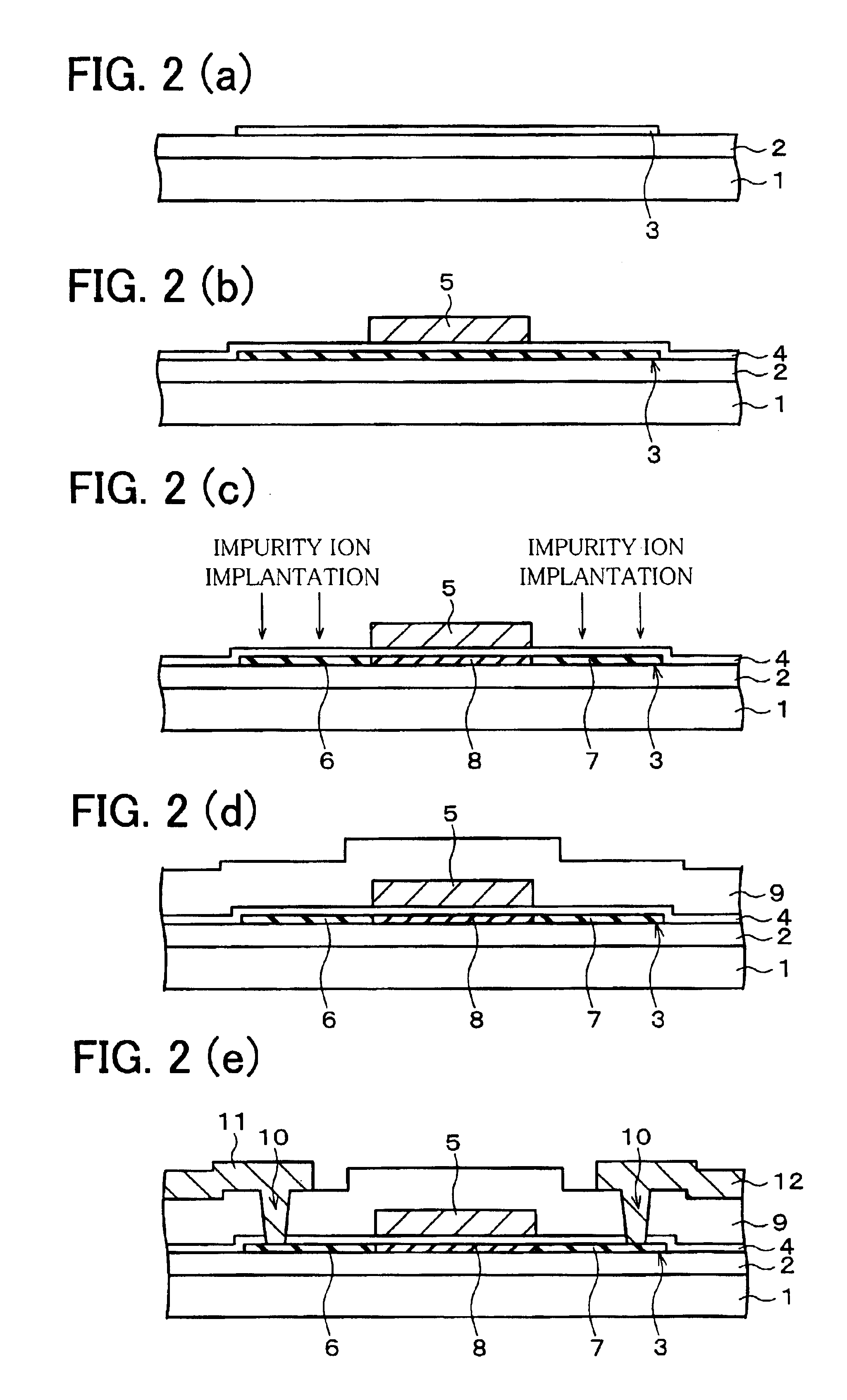
[0067]The following will explain an example of the TFT 20 of FIG. 1, with reference to FIGS. 1, 2(a) through 2(e). Here, a single gate structure is combined with the division of the channel region width.

[0068]FIG. 2(e) is a cross-sectional view of a TFT in which the single gate structure is adopted in the arrangement of the TFT 20, corresponding to a cross-sectional view taken on line A—A of FIG. 1. The TFT is an NMOS transistor used for a driving circuit element of a liquid crystal display device, for example.

[0069]In the TFT, on an entire top surface of a transparent insulating substrate 1 made of silicon dioxide, etc., a first interlayer insulating film having a thickness of approximately 200 μm to 500 μm is formed with an insulating film such as silicon oxide (SiO2) and HTO (High Temperature Oxide).

[0070]On the first interlayer insulating film 2, a plurality of (six, in this example) divided semiconductor layers 3 respectively having a thickness of approximately 50 nm to 150 nm ...

example 2

[0086]The following will explain another example of the TFT 20 as shown in FIG. 1, with reference to FIGS. 1, 3(a), and 3(b). Here, the LDD structure is combined with the division of the channel region width.

[0087]In the TFT of the present example, the LDD structure is adopted in the arrangement of the TFT 20. The TFT is an NMOS transistor used for a driving circuit element of a liquid crystal display device, for example.

[0088]The TFT of the present example having the LDD structure differs from the TFT of example 1 in that a low impurity region is provided between the divided source regions 6 and the divided channel regions 8, and between the divided drain regions 7 and the divided channel regions 8 (see FIG. 3(b)). By using the LDD structure, the electric field intensity is reduced between the channel and the drain, thereby achieving an effect of reducing the deterioration of the TFT characteristics due to hot carriers.

[0089]The manufacturing steps of the TFT 20 having the LDD stru...

example 3

[0096]The following will explain a further example of the TFT 20 as shown in FIG. 1, with reference to FIGS. 1, and 4(a) through 4(c). Here, the GOLD structure is combined with the division of the channel region width.

[0097]In the TFT of the present example, the GOLD structure is adopted in the arrangement of the TFT 20. The TFT is an NMOS transistor used for a driving circuit element of a liquid crystal display device, for example.

[0098]The TFT of the present example having the GOLD structure differs from the TFT of example 1 in that an overlap region 15a and an offset region 15b which are low impurity regions 15 are provided between the divided source regions 6 and the divided channel regions 8, and between the divided drain regions 7 and the divided channel regions 8 (see FIG. 4(c)). By using the GOLD structure, the electric field intensity is reduced between the channel and the drain, thereby achieving an effect of reducing the deterioration of the TFT characteristics due to hot...


PUM


Abstract

A thin film transistor of the present invention is provided with (i) a plurality of divided channel regions formed under a gate electrode, and (ii) divided source regions and divided drain regions between which each of the divided channel regions is sandwiched, the divided source regions being connected with one another, and the divided drain regions being connected with one another. Here, the divided channel regions are so arranged that a spacing between the divided channel regions is smaller than a channel divided width which is a width of one divided channel region, the channel divided width is not more than 50 μm, and the spacing is not less than 3 μm. With this arrangement, it is possible to provide a thin film transistor capable of obtaining reliability with reducing the variation in threshold voltage by reducing the self-heating at the channel regions, as well as capable of reducing the increase of a layout area.

Description

FIELD OF THE INVENTION[0001]The present invention relates to a Thin Film Transistor (TFT) capable of preventing deterioration in characteristics; a method of manufacturing the same; and a liquid crystal display device using the same.BACKGROUND OF THE INVENTION[0002]In recent years, there is a growing demand for liquid crystal projectors as high definition display devices used for presentation, home theater, etc. The liquid crystal projector, which is a kind of a liquid crystal display device, is expected to be used widely as household devices such as a rear projection television, so that it is crucial for the liquid crystal projector to obtain reliability sufficient for consumer use.[0003]In the liquid crystal projector, a TFT is used in a drive circuit section of a liquid crystal panel that composes the liquid crystal projector. Operation of the TFT, however, generates a variation in threshold voltage and a resultant lowering of driving current, thereby causing a serious problem in...

Claims


Application Information

Patent Timeline
Patent Type & Authority Patents(United States)
IPC IPC(8): H01L21/02H01L29/66H01L21/336H01L29/786
CPCH01L29/66757H01L29/66772H01L29/78627H01L29/78696H01L29/78621H01L2029/7863G02F1/136
Inventor MITANI, MASAHIROFUKUSHIMA, YASUMORI
Owner SHARP KK
Why Eureka
Try Eureka