Semiconductor memory device with a page mode

a memory device and memory technology, applied in the direction of information storage, static storage, digital storage, etc., can solve the problems of increasing the layout area of the transistor or wiring, increasing the peak current value, etc., and achieve the effect of increasing the layout area and minimizing the peak curren

Inactive Publication Date: 2007-02-20
RENESAS ELECTRONICS CORP
View PDF3 Cites 9 Cited by
  • Summary
  • Abstract
  • Description
  • Claims
  • Application Information

AI Technical Summary

Benefits of technology

[0007]It is an object of this invention to provide a semiconductor memory device having a page mode reading function that minimizes a peak current and an increase in layout area.
[0012]Therefore, a semiconductor memory device that minimizes a peak current at the time of page mode reading and an increase in layout area of a circuit that achieves the page mode reading function is obtained.

Problems solved by technology

However, a word length increase of page mode involves an increase in the number of simultaneously activated sense amplifiers and also an increase in memory capacity of a latch for temporarily storing data, resulting in problems such as an increase in peak current value and an increase in layout area of a transistor or wiring.

Method used


Image

  • Semiconductor memory device with a page mode
  • Semiconductor memory device with a page mode
  • Semiconductor memory device with a page mode

Examples


Embodiment Construction
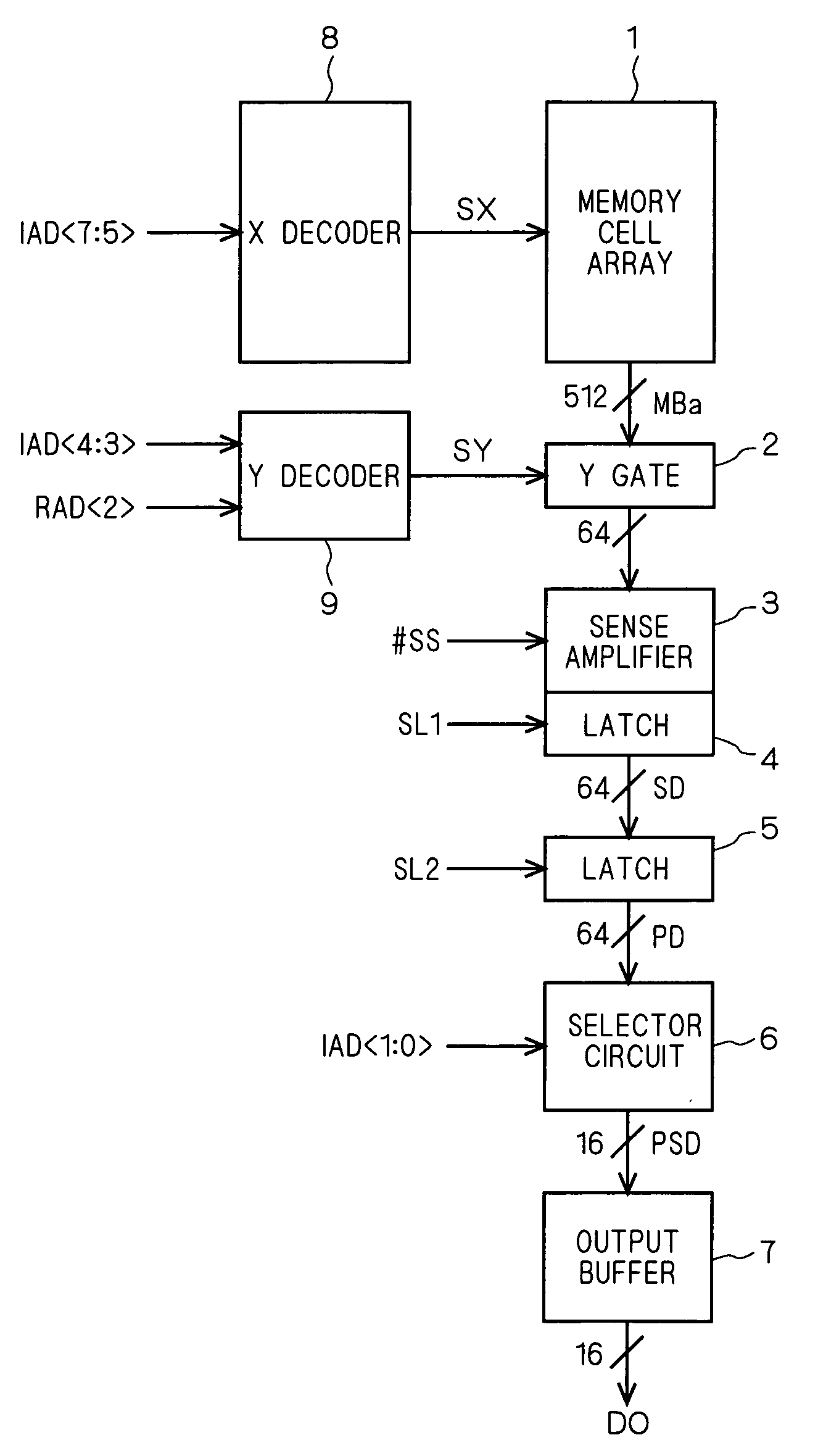
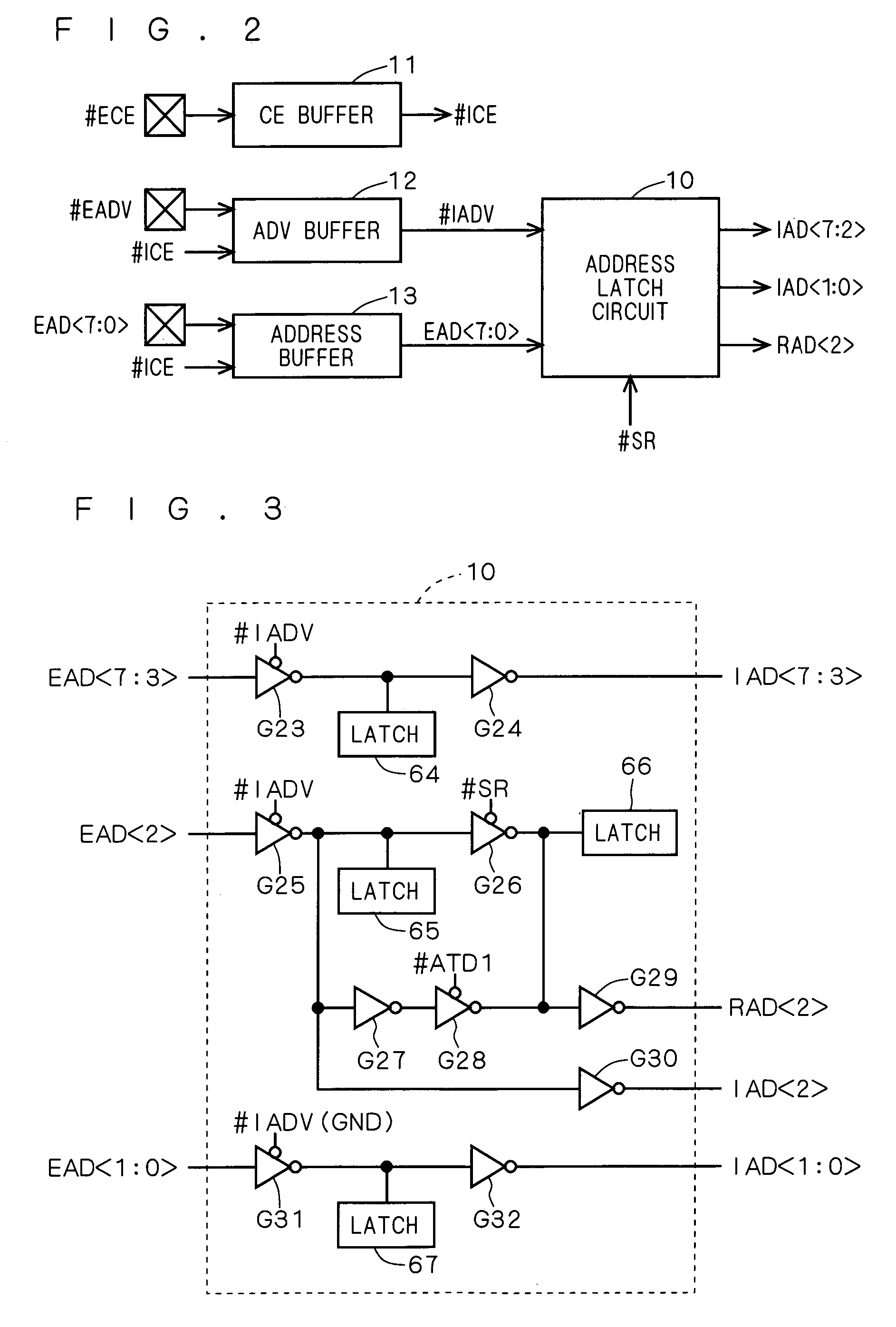
[0038]

[0039]In a semiconductor memory device having the page mode reading function of a prescribed page length, a page mode of a substantial page length being several times as long (hereinafter referred to as “sequential page mode”) would be attained by sequentially operating the page mode reading function multiple times, which would ensure high-speed data transmission while suppressing the above-mentioned problems including the increase in peak current value and the increase in layout area. However, this has conventionally been far from a reality due to extremely complicated operations required for automatically keeping the page mode reading function inside during a page mode reading operation that essentially operates asynchronously with an access request from outside. Especially hard to attain is consistency with redundant data. This invention has been made for the purpose of solving such problem.

[0040]This invention is applicable not only to volatile semiconductor memory devices...


PUM


Abstract

A sense amplifier and a latch for sense data output the former 4 words of sense data to a latch for page data, and during a page mode reading period of the former 4 words of data as external data by the latch for page data, a selector circuit and an output buffer, perform a sense amplifying operation and a latch operation on the latter 4 words of memory cell information output from a Y gate under control of a sense signal and a latch signal.

Description

BACKGROUND OF THE INVENTION[0001]1. Field of the Invention[0002]This invention relates to semiconductor memory devices having a page mode reading function.[0003]2. Description of the Background Art[0004]In semiconductor memory devices such as DRAMs in which memory cells per se have no logic outputting function of “H” and “L” levels, a sense amplifying operation is required in order to detect and amplify data stored in the memory cells and convert the data into logical value (“H” and “L”). As performing the sense amplifying operation on a word-by-word basis will extremely delay access to data, a page mode reading function is widely used in which data recorded in a plurality of words of memory cells are simultaneously read (including the sense amplifying operation) and temporarily stored in a latch, so that the data are accessible with read time from the latch the second and subsequent times. Semiconductor memory devices having the page mode reading function are disclosed, for example...

Claims


Application Information

Patent Timeline
Patent Type & Authority Patents(United States)
IPC IPC(8): G11C7/10G11C29/00G11C7/00G11C8/18G11C11/401G11C5/00G11C8/06G11C8/12
CPCG11C8/12G11C8/06
Inventor KUBO, TAKASHI
Owner RENESAS ELECTRONICS CORP
Why Eureka
Try Eureka