Apparatus for adjusting input capacitance of semiconductor device and fabricating method

a technology of input capacitance and fabricating method, which is applied in the direction of digital transmission, instruments, baseband system details, etc., can solve the problems of increasing the overall size reducing the operation and performance of the semiconductor device, etc., and achieves the effect of not increasing the layout area of the semiconductor memory devi

Inactive Publication Date: 2005-06-21
SK HYNIX INC
View PDF15 Cites 9 Cited by
  • Summary
  • Abstract
  • Description
  • Claims
  • Application Information

AI Technical Summary

Benefits of technology

[0021]As mentioned in the above description, a fine-adjustment circuit and a method of fabricating the fine-adjustment circuit thereof according to the p

Problems solved by technology

However, even if all the input parts have been designed to provide the desired input capacitance for the semiconductor device, the input capacitance considered outside a chip is different in accordance with input pins which thwarts this effort for obtaining the

Method used


Image

  • Apparatus for adjusting input capacitance of semiconductor device and fabricating method
  • Apparatus for adjusting input capacitance of semiconductor device and fabricating method
  • Apparatus for adjusting input capacitance of semiconductor device and fabricating method

Examples


Embodiment Construction

[0031]Reference will now be made in detail to the preferred embodiments of the present invention, examples of which are illustrated in the accompanying drawings. Where possible, the same reference numerals will be used to illustrate like elements throughout the specification.

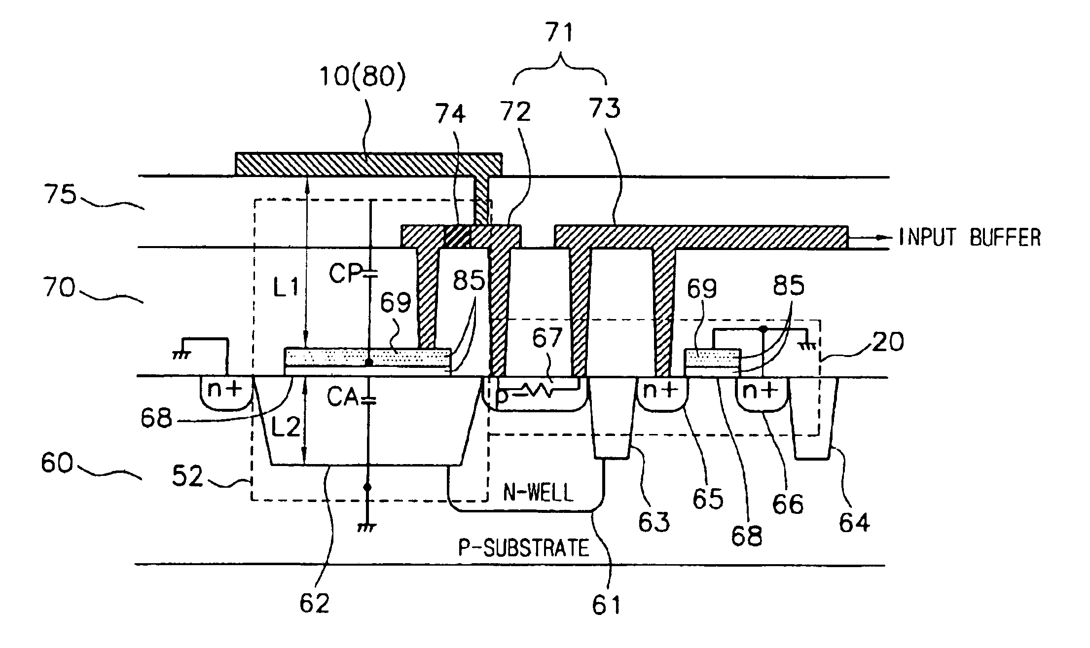
[0032]In the present invention, an input capacitance of a semiconductor device is finely adjusted without having to increase the layout area of the semiconductor device. This is accomplished by providing a capacitor composed of a poly layer, a device isolation layer and a p-type substrate and formed under an input pad of the semiconductor device.

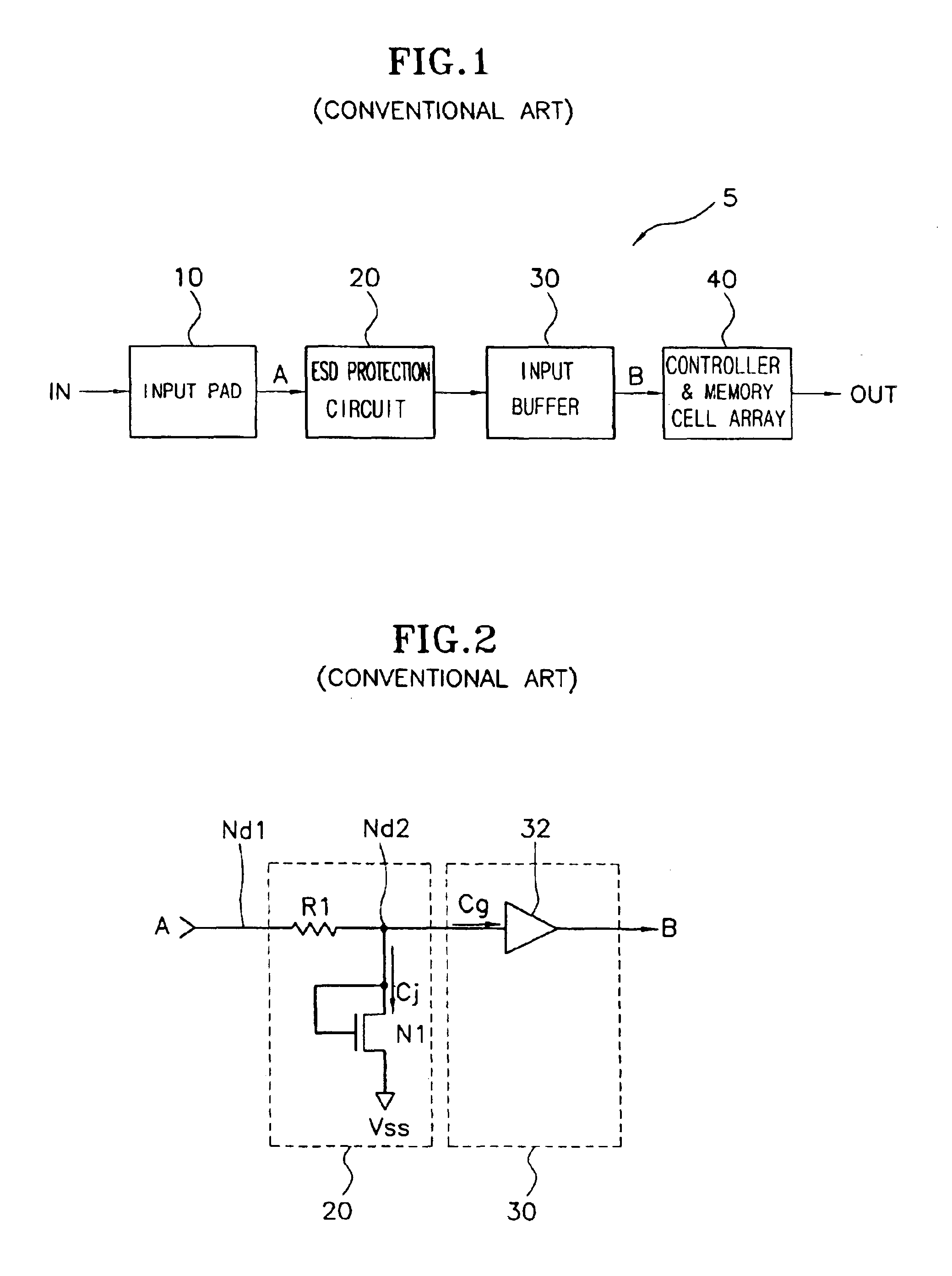
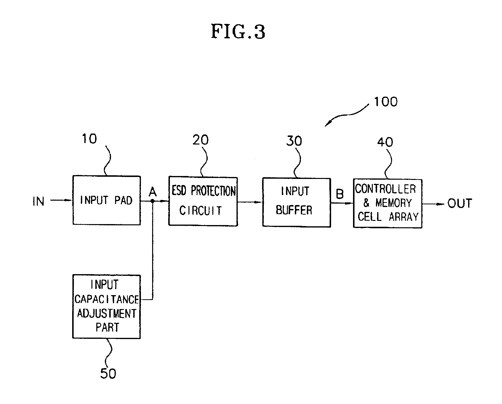
[0033]Particularly, FIG. 3 illustrates a block diagram of an input part 100 of a semiconductor device according to one embodiment of the present invention. Referring to FIG. 3, the input part 100 includes an input pad 10 for receiving an input signal IN from an external source and transmitting the input signal IN as an output signal A, an ESD protection circuit 20 for pr...


PUM


Abstract

An apparatus for finely adjusting the input capacitance of a semiconductor device and a method of fabricating the apparatus are disclosed. The invention adjusts finely the input capacitance without increasing a layout area of the device by using a capacitor constructed with a poly layer/device isolation layer/P-type substrate. The poly layer is formed on an unnecessary space provided by the device isolation layer under an input pad.

Description

CROSS-REFERENCE[0001]The present application is a continuation of U.S. patent application Ser. No. 10 / 006,566 filed on Dec. 10, 2001 (now U.S. Pat. No. 6,741,114 B2 issued May 25, 2004) for which priority is claimed under 35 U.S.C. § 120; and the present application claims priority of patent application Ser. No. 2001-25523 filed in Republic of Korea on May 10, 2001, under 35 U.S.C. § 119. The entire contents of each of these applications are herein fully incorporated by reference.BACKGROUND OF THE INVENTION[0002]1. Field of the Invention[0003]The present invention relates to an apparatus for adjusting finely the input capacitance of a semiconductor device without increasing a layout area of the device, and to a method of fabricating the apparatus.[0004]2. Discussion of the Related Art[0005]FIG. 1 illustrates a block diagram of an input part 5 of a semiconductor memory device according to a related art. As shown in FIG. 1, the input part 5 includes an input pad 10 for transmitting an...

Claims


Application Information

Patent Timeline
IPC IPC(8): G11C5/00H01L27/04H01L23/60H01L23/64H01L27/02H04L25/02
CPCG11C5/005H01L23/60H01L23/642H01L27/0251H04L25/0278H01L2924/0002H04L25/0292H01L2924/00H01L27/04
Inventor KIM, TAEK SEUNG
Owner SK HYNIX INC
Why Eureka
Try Eureka