Manufacturing method of optical waveguide device and optical waveguide device obtained thereby

a technology of optical waveguide and manufacturing method, which is applied in the direction of optical waveguide light guide, instruments, photomechanical treatment, etc., can solve the problems of increasing the propagation loss of light propagating inside the core b, b>, suppressing the surface roughening of the side surfaces, and preventing the increase in the total thickness of the optical waveguide device

Active Publication Date: 2013-09-17
NITTO DENKO CORP
View PDF18 Cites 0 Cited by
  • Summary
  • Abstract
  • Description
  • Claims
  • Application Information

AI Technical Summary

Benefits of technology

[0009]In view of the foregoing, it is an object of the present invention to provide a manufacturing method of an optical waveguide device capable of suppressing the surface roughening of core side surfaces of an optical waveguide when the optical waveguide is formed on a surface of a PET substrate, and an optical waveguide device obtained thereby.
[0014]In the manufacturing method of the optical waveguide device according to the present invention, when the PET substrate which forms the optical waveguide is the above-mentioned colored-layer-coated substrate (A) (a colored-layer-coated PET substrate), the under cladding layer is formed on the front surface (the surface on which the colored layer is not formed) of the colored-layer-coated PET substrate, and the photosensitive resin layer for the formation of the cores is formed thereon. Thereafter, the irradiation light is directed toward this photosensitive resin layer to expose the photosensitive resin layer in a predetermined pattern to the irradiation light, thereby forming exposed portions of the photosensitive resin layer into the cores. In this step of forming the cores, the irradiation light transmitted through the photosensitive resin layer for the formation of the cores and through the under cladding layer enters the above-mentioned colored-layer-coated PET substrate portion. Although the irradiation light impinges upon a lubricant material and the like contained in the PET substrate portion so that the path thereof is made irregular, most of the irradiation light reaches the bottom surface of the above-mentioned PET substrate portion. Since the colored layer of the color that absorbs the irradiation light is formed on the back surface of the above-mentioned PET substrate portion, most of the irradiation light that has reached the bottom surface of the above-mentioned PET substrate portion is absorbed by the above-mentioned colored layer, and there is little irradiation light reflected from the bottom surface of the above-mentioned PET substrate portion. This significantly reduces the irradiation light reflected from the bottom surface of the above-mentioned PET substrate portion, transmitted through the under cladding layer obliquely upwardly from below, and reaching the photosensitive resin layer for the formation of the cores. As a result, there is little irradiation light which causes the future side surfaces of the cores to become roughened surfaces because of the exposure of the future side surfaces thereto in the photosensitive resin layer for the formation of the cores. This effectively suppresses the surface roughening of the side surfaces of the cores.
[0015]On the other hand, when the PET substrate which forms the optical waveguide is the above-mentioned colored substrate (B) (a colored PET substrate), most of the irradiation light entering the above-mentioned colored PET substrate is absorbed in the above-mentioned colored PET substrate in the above-mentioned core formation step. This significantly reduces the irradiation light reflected from the bottom surface of the above-mentioned colored PET substrate, transmitted through the under cladding layer obliquely upwardly from below, and reaching the photosensitive resin layer for the formation of the cores. As a result, there is little irradiation light which causes the future side surfaces of the cores to become roughened surfaces because of the exposure of the future side surfaces thereto in the photosensitive resin layer for the formation of the cores. This effectively suppresses the surface roughening of the side surfaces of the cores. Additionally, when the PET substrate which forms the optical waveguide is the above-mentioned colored PET substrate (B), the colored PET substrate itself absorbs the irradiation light, as mentioned earlier, to cause little irradiation light to be reflected therefrom. This eliminates the need to provide a new layer for the absorption of the irradiation light to offer the advantage of preventing the increase in the total thickness of the optical waveguide device.
[0016]The optical waveguide device according to the present invention is that obtained by the above-mentioned manufacturing method. Thus, the surface roughening of the side surfaces of the cores is effectively suppressed. This reduces the propagation losses of light propagating inside the cores.
[0017]In particular, when the color that absorbs the above-mentioned irradiation light is black, the property of absorbing the irradiation light is excellent, and the surface roughening of the side surfaces of the cores is more effectively suppressed. This further reduces the propagation losses of light propagating inside the cores in the obtained optical waveguide device.

Problems solved by technology

An optical waveguide having such cores 30 presents a problem in that the propagation losses of light propagating inside the cores 30 are increased. FIG. 5B is a view drawn based on a photograph in perspective of a core 30 enclosed with a circle C of FIG. 5A which is magnified 700 times with an electron microscope.

Method used


Image

  • Manufacturing method of optical waveguide device and optical waveguide device obtained thereby
  • Manufacturing method of optical waveguide device and optical waveguide device obtained thereby
  • Manufacturing method of optical waveguide device and optical waveguide device obtained thereby

Examples


##ventive example 1

INVENTIVE EXAMPLE 1

Colored-Layer-Coated PET Substrate

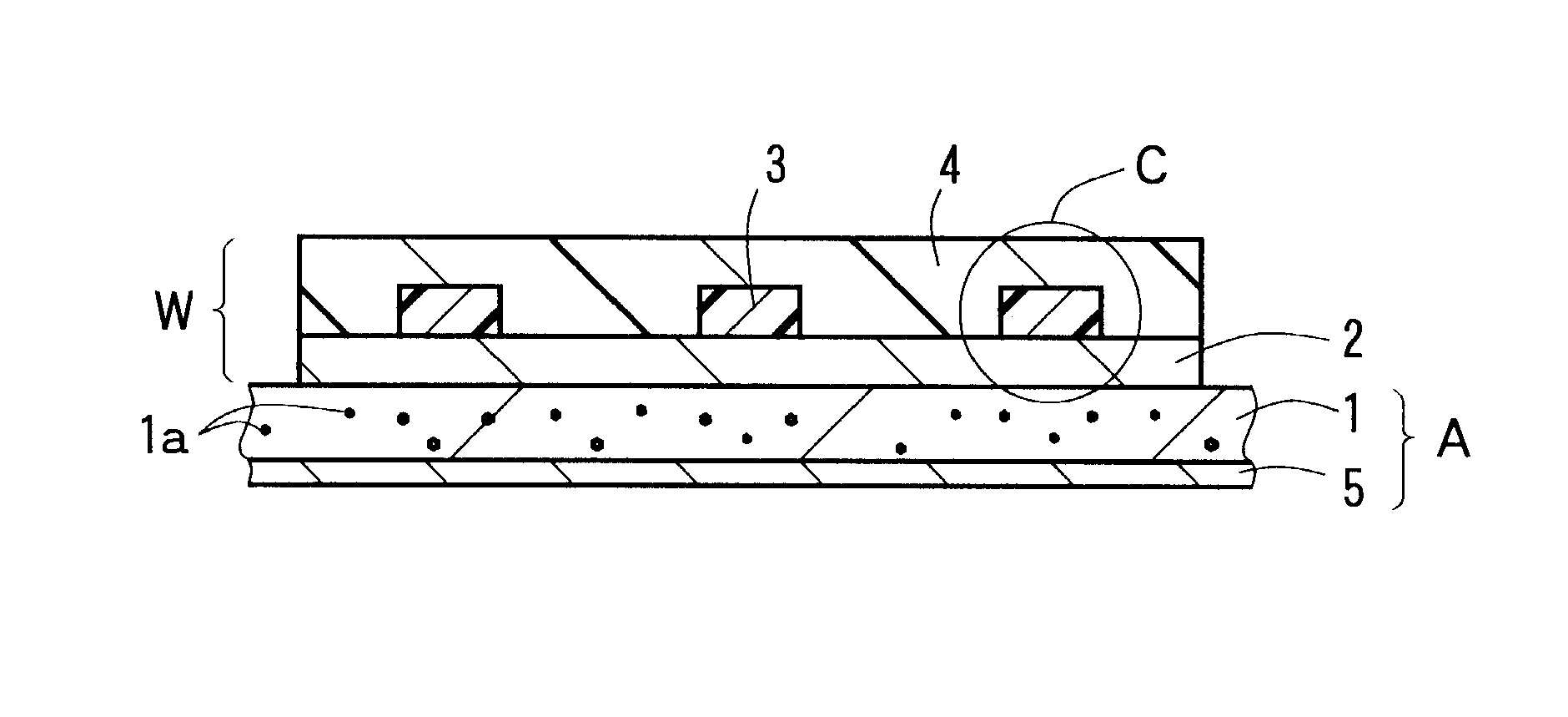
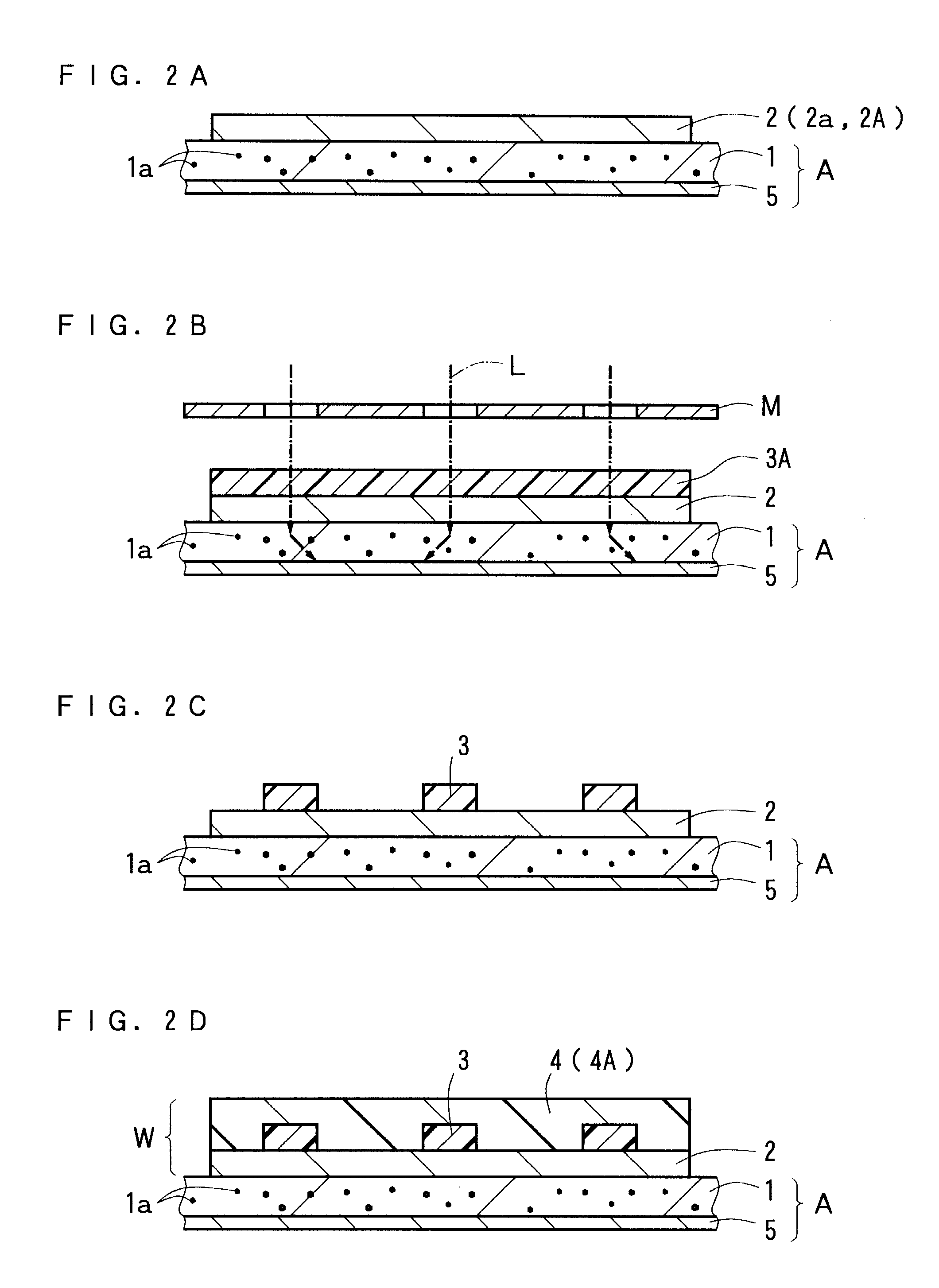
[0045]A colorless transparent PET substrate (manufactured by Toray Industries, Inc., Type T60, under the product designation 188, and having a thickness of 188 μm) was prepared. Then, black alcohol-based ink was applied to one surface (the back surface) of the PET substrate by using an oil-based marking pen to form a colored layer having a thickness of 50 nm.

Material for Formation of Under Cladding Layer and Over Cladding Layer

[0046]A material for formation of an under cladding layer and an over cladding layer was prepared by mixing 35 parts by weight of bisphenoxyethanol fluorene glycidyl ether (component A) represented by the following general formula (1), 40 parts by weight of 3′,4′-epoxycyclohexyl methyl-3,4-epoxycyclohexane carboxylate which is an alicyclic epoxy resin (CELLOXIDE 2021P manufactured by Daicel Chemical Industries, Ltd.) (component B), 25 parts by weight of (3′4′-epoxycyclohexane)methyl-3′,4′-epoxycyclohexyl-car...

##ventive example 2

INVENTIVE EXAMPLE 2

[0052]An optical waveguide device was manufactured by forming the under cladding layer, the cores and the over cladding layer directly on the front surface of a black transparent colored PET substrate (manufactured by Mitsubishi Plastics, Inc., Type Z608E, under the product designation U07-17 MB, and having a thickness of 25 μm) in a manner similar to that in Inventive Example 1 described above.


PUM


Abstract

A manufacturing method of an optical waveguide device and an optical waveguide device obtained thereby. An under cladding layer is formed on the front surface of a colored-layer-coated PET substrate including a PET substrate portion and a colored layer of a color that absorbs irradiation light and formed on the back surface of the PET substrate portion, and then a photosensitive resin layer for the formation of cores is formed thereon. In forming the cores, when the irradiation light reaches the bottom surface of the PET substrate portion, most of the irradiation light is absorbed by the colored layer, so that there is little irradiation light reflected from the bottom surface of the PET substrate portion. This significantly reduces the irradiation light reflected diffusely from the PET substrate portion and reaching the photosensitive resin layer to thereby effectively suppress the surface roughening of the side surfaces of the cores.

Description

RELATED APPLICATIONS[0001]This application claims the benefit of U.S. Provisional Application No. 61 / 101,823, filed Oct. 1, 2008, which is hereby incorporated by reference.BACKGROUND OF THE INVENTION[0002]1. Field of the Invention[0003]The present invention relates to a manufacturing method of an optical waveguide device for widespread use in optical communications, optical information processing and other general optics, and an optical waveguide device obtained thereby.[0004]2. Description of the Related Art[0005]In general, an optical waveguide for an optical waveguide device is constructed such that cores serving as a passageway for light are formed in a predetermined pattern on a surface of an under cladding layer, and such that an over cladding layer is formed so as to cover the cores. Such an optical waveguide is typically formed on a surface of a substrate such as a metal substrate and the like, and is manufactured together with the substrate to provide an optical waveguide d...

Claims


Application Information

Patent Timeline
Patent Type & Authority Patents(United States)
IPC IPC(8): G02B6/10
CPCG02B6/1221G02B6/138G02B6/13
Inventor HIKITA, TAKAMIFUJISAWA, JUNICHISHIMIZU, YUSUKE
Owner NITTO DENKO CORP
Why Eureka
Try Eureka