

Manufacturing method of optical waveguide device
a manufacturing method and technology of optical waveguide, applied in the direction of photomechanical equipment, instruments, originals for photomechanical treatment, etc., can solve problems such as diffuse reflection, and achieve the effect of suppressing surface roughening of side surfaces and preventing the increase of the total thickness of the optical waveguide devi
- Summary
- Abstract
- Description
- Claims
- Application Information
AI Technical Summary
Benefits of technology
Problems solved by technology
Method used
Image

Examples
##ventive example 1
INVENTIVE EXAMPLE 1
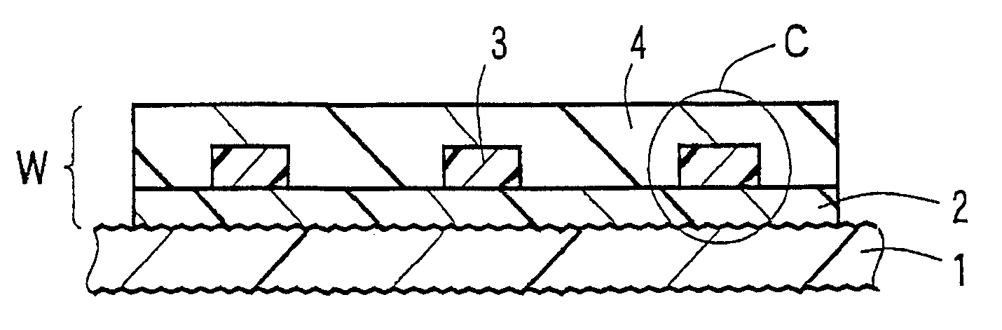
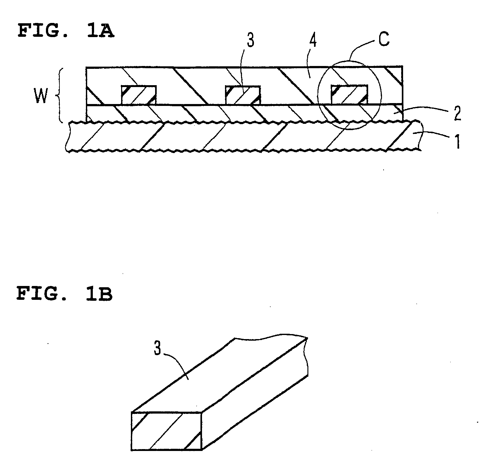
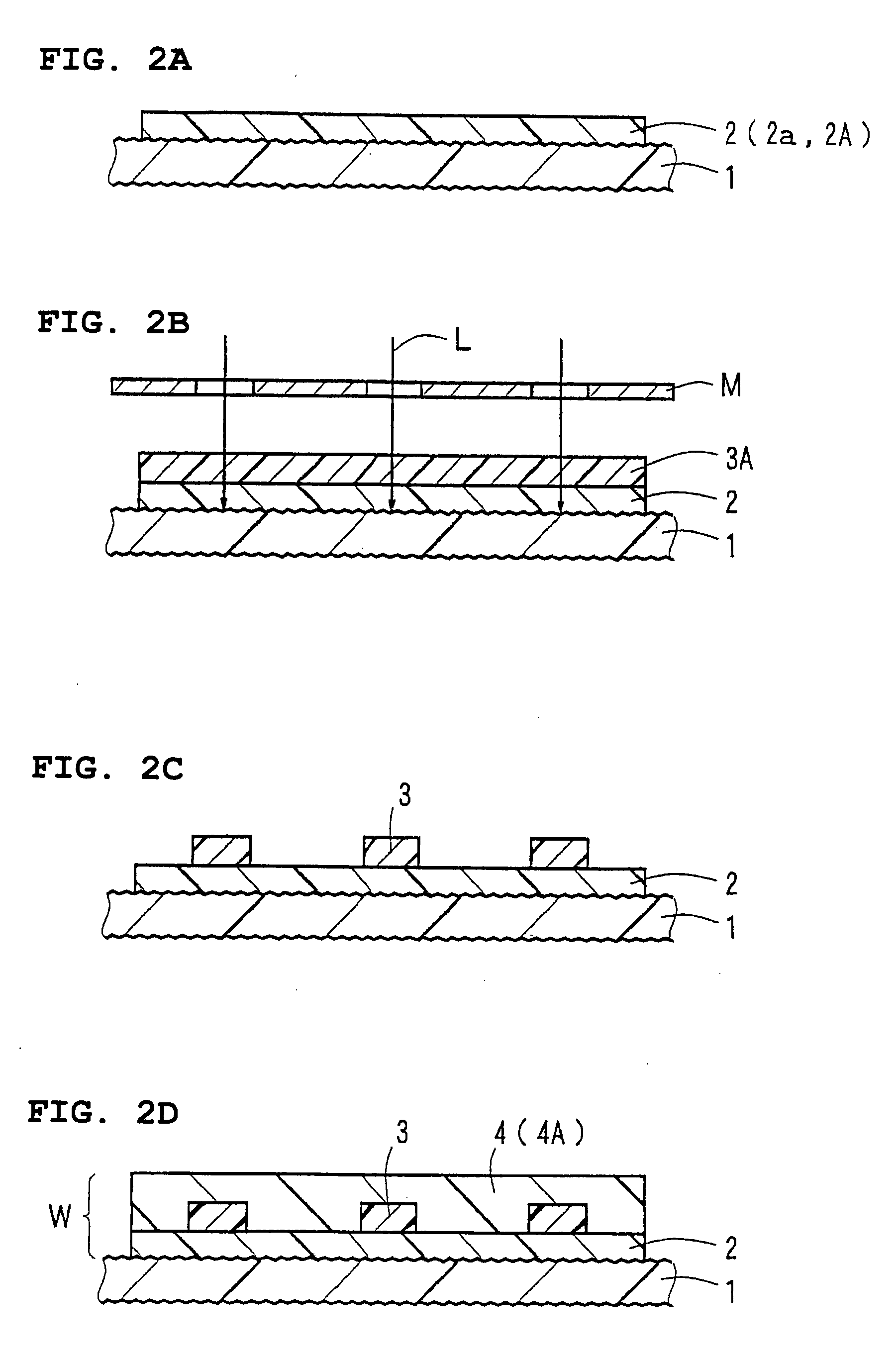
Substrate
[0035]A PMMA substrate [manufactured by Mitsubishi Rayon Co., Ltd., and having a thickness of 2000 μm and an arithmetic mean roughness (Ra) of 1.5 μm] was prepared.
Material for Formation of Under Cladding Layer and Over Cladding Layer
[0036]A material for formation of an under cladding layer and an over cladding layer was prepared by mixing 35 parts by weight of bisphenoxyethanol fluorene glycidyl ether (component A) represented by the following general formula (1), 40 parts by weight of 3′,4′-epoxycyclohexyl methyl-3,4-epoxycyclohexane carboxylate which is an alicyclic epoxy resin (CELLOXIDE 2021P manufactured by Daicel Chemical Industries, Ltd.) (component B), 25 parts by weight of (3′4′-epoxycyclohexane)methyl-3′,4′-epoxycyclohexyl-carboxylate (CELLOXIDE 2081 manufactured by Daicel Chemical Industries, Ltd.) (component C), and 2 parts by weight of a 50% propione carbonate solution of 4,4′-bis[di(β-hydroxyethoxy)phenylsulfinio]phenyl-sulfide-bis-hexafluo...
PUM
| Property | Measurement | Unit |
|---|---|---|
| Ra | aaaaa | aaaaa |
| thickness | aaaaa | aaaaa |
| wavelength | aaaaa | aaaaa |
Abstract
Description
Claims
Application Information