

Method for manufacturing multi-gate transistor device
a transistor and multi-gate technology, applied in the direction of semiconductor devices, basic electric elements, electrical appliances, etc., can solve the problems of inability to repair damage caused by ion implantation inability to provide stable high-k insulating layer, etc., to achieve improved multi-gate transistor device performance, improved mobility in the channel region, and reduced manufacturing costs
- Summary
- Abstract
- Description
- Claims
- Application Information
AI Technical Summary
Benefits of technology
Problems solved by technology
Method used
Image

Examples
Embodiment Construction
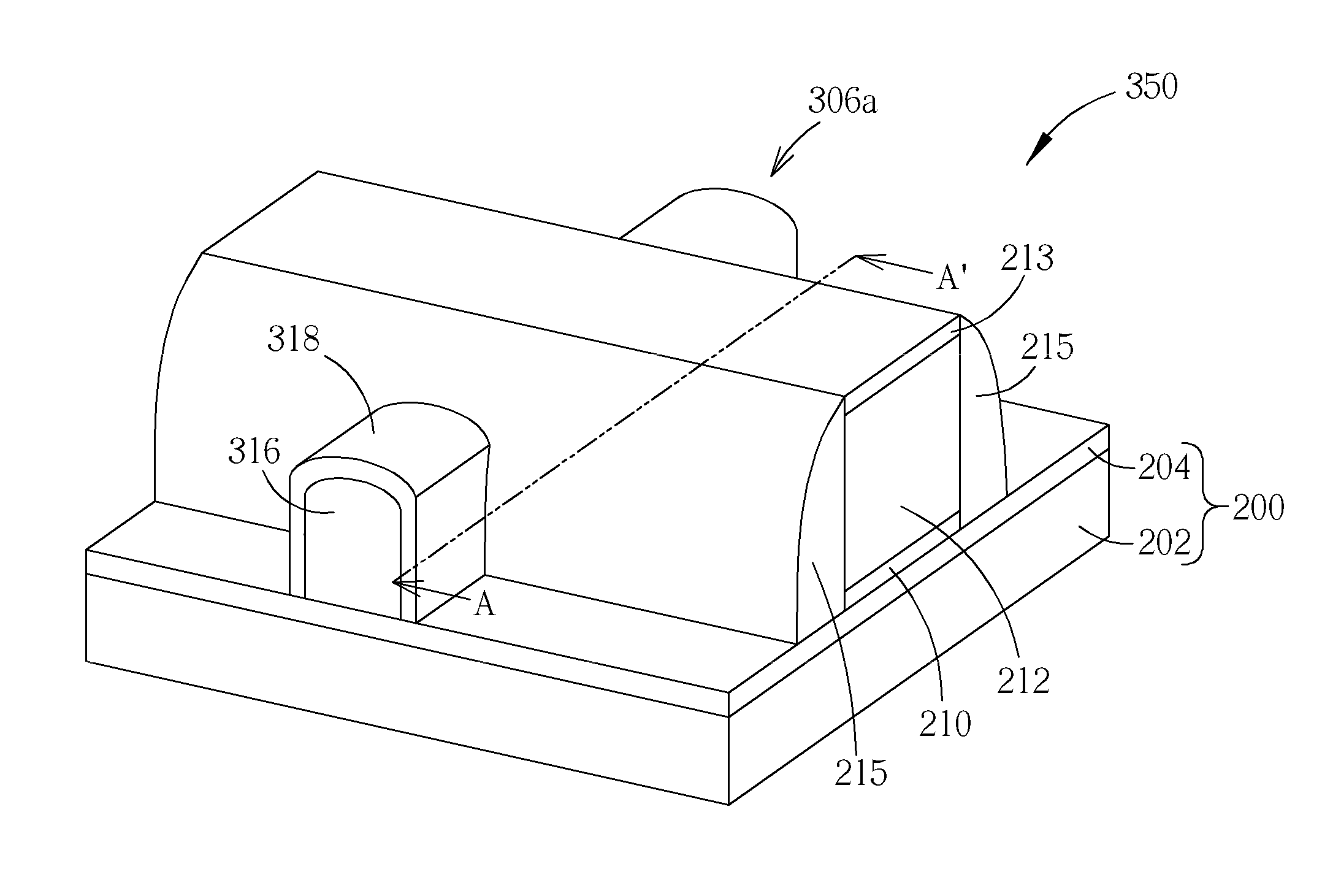
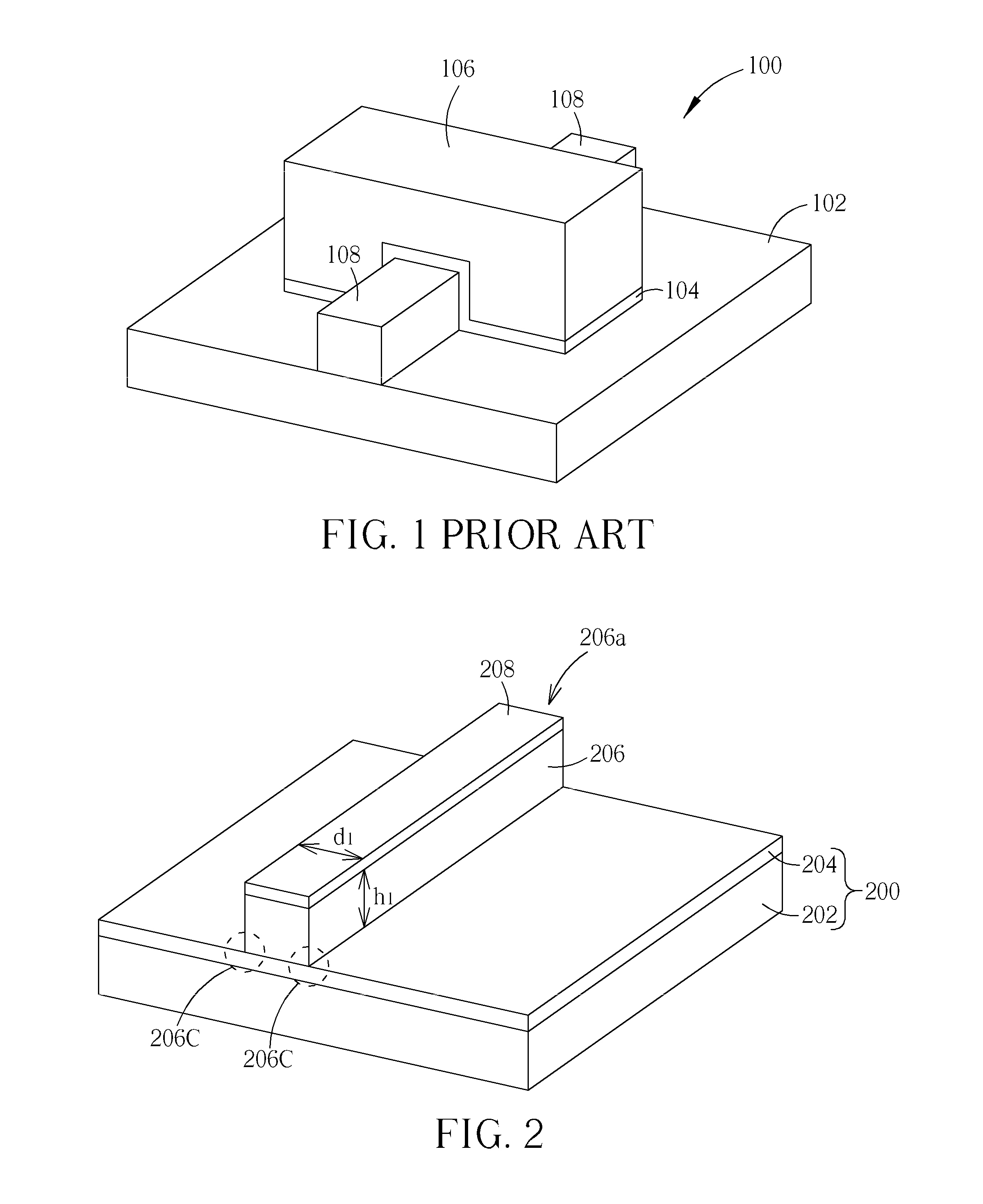
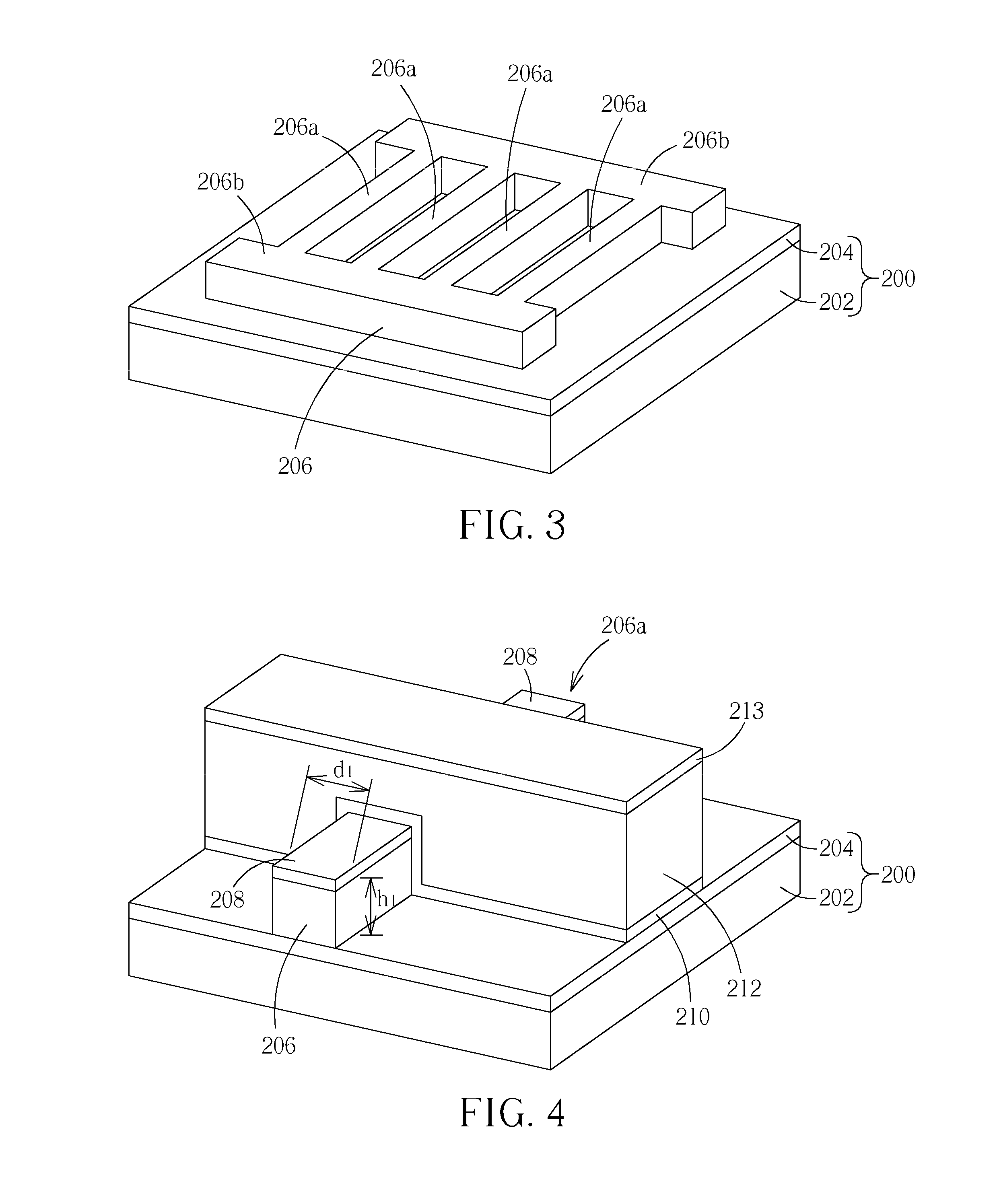
[0014]Please refer to FIGS. 2-7, which are schematic drawings illustrating the method for manufacturing a multi-gate transistor device provided by a first preferred embodiment of the present invention. As shown in FIG. 2, the preferred embodiment first provides a semiconductor substrate 200. The semiconductor substrate 200 can include a silicon-on-insulator (SOI) substrate. It is well-known to those skilled in the art that the SOI substrate upwardly includes a silicon substrate 202, a bottom oxide (BOX) layer 204, and a semiconductor layer (not shown) such as a single crystalline silicon layer formed on the BOX layer 204. However, for providing superior ground connection and thermal dissipation and for reducing interference and cost, the semiconductor substrate 200 provided by the preferred embodiment also can include a bulk silicon substrate.
[0015]Please still refer to FIG. 2. Next, a patterned hard mask 208 for defining at least a fin of a multi-gate transistor device is formed on...
PUM
 Abstract
Description
Claims
Application Information