Semiconductor device, liquid discharge head, liquid discharge cartridge, and liquid discharge apparatus

a technology of semiconductor devices and liquid discharge cartridges, applied in the direction of printing, other printing apparatus, etc., can solve the problems of achieve the effect of increasing the width of the line running from the bonding pad to the respective segment, increasing the division count of the conductive line connected to the power supply pad, and increasing the printhead siz

Active Publication Date: 2013-10-22
CANON KK
View PDF9 Cites 4 Cited by
  • Summary
  • Abstract
  • Description
  • Claims
  • Application Information

AI Technical Summary

Benefits of technology

[0005]In the printhead disclosed in Japanese Patent Laid-Open No. 2005-104142, when the printhead is prolonged by increasing the number of heaters arranged on a semiconductor substrate, the division count of a conductive line connected to the power supply pad increases. The widths of lines running from the bonding pad to respective segments cumulatively increase. The wiring layout requires a large area, increasing the printhead size. One aspect of the present invention provides a technique for suppressing enlargement of the wiring area while suppressing variations of line resistances up to respective segments.

Problems solved by technology

The wiring layout requires a large area, increasing the printhead size.

Method used


Image

  • Semiconductor device, liquid discharge head, liquid discharge cartridge, and liquid discharge apparatus
  • Semiconductor device, liquid discharge head, liquid discharge cartridge, and liquid discharge apparatus
  • Semiconductor device, liquid discharge head, liquid discharge cartridge, and liquid discharge apparatus

Examples


first embodiment

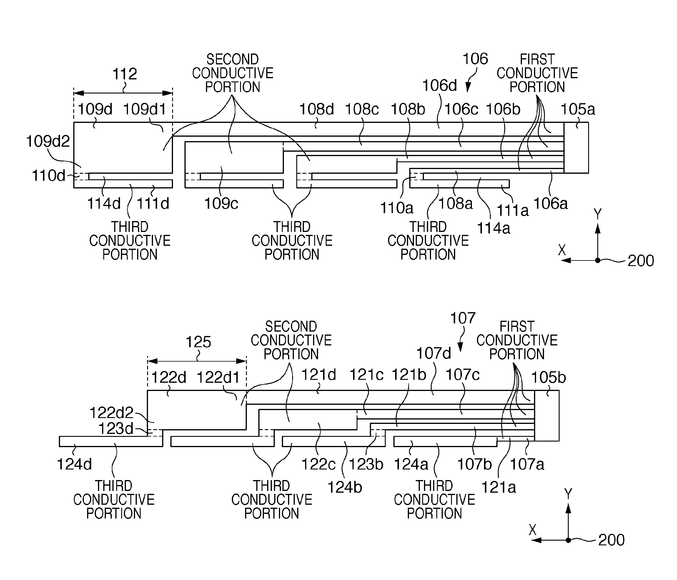
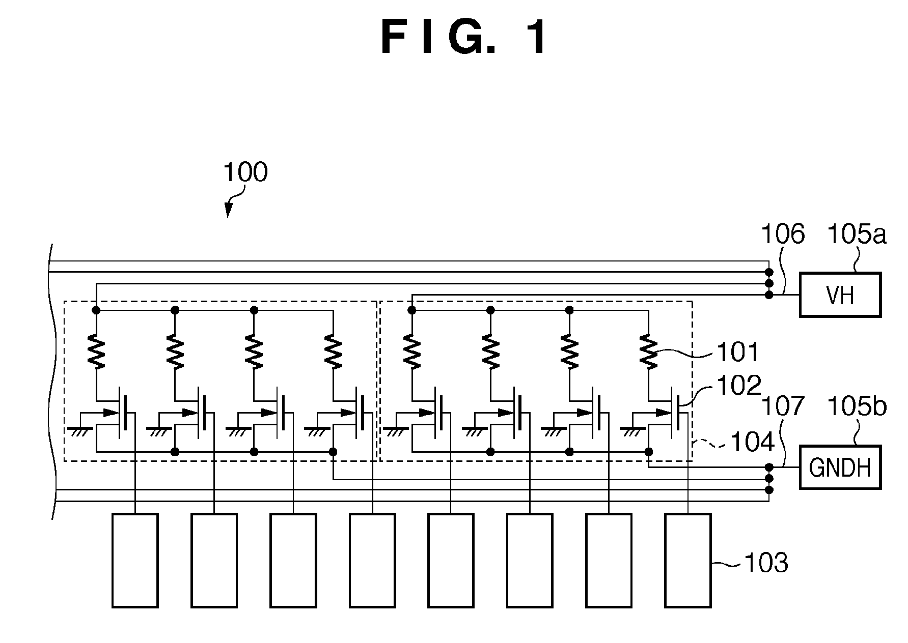
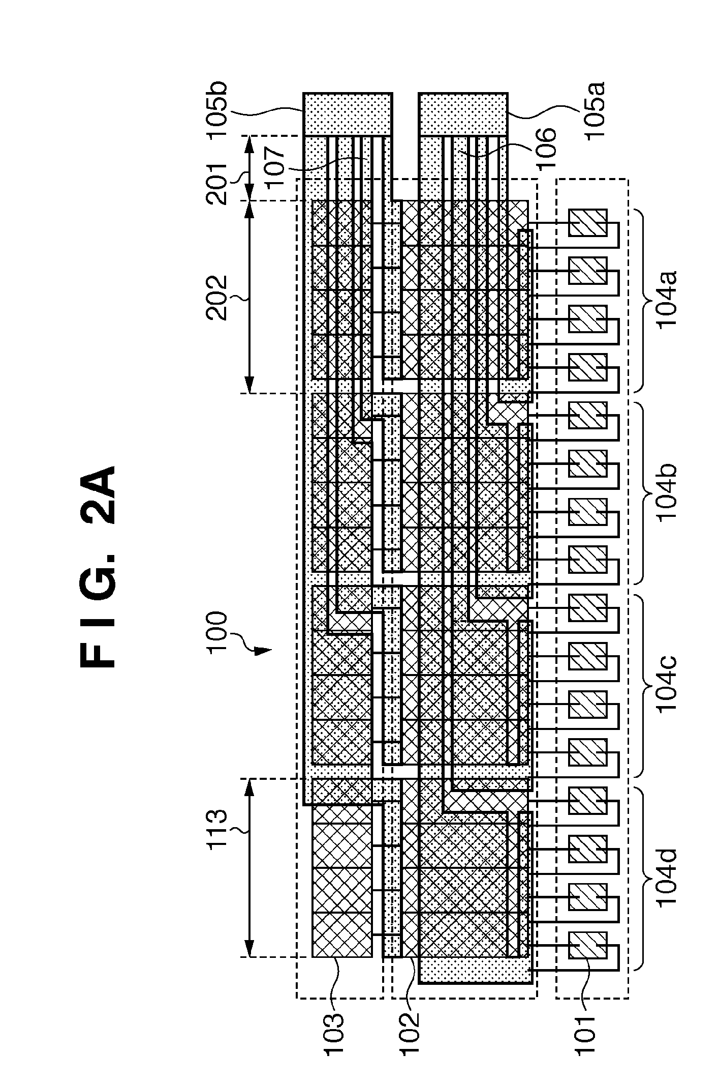
[0016]The circuit arrangement of a semiconductor device 100 according to the first embodiment will be exemplified with reference to FIG. 1. The semiconductor device 100 can be used to control an inkjet printhead. The semiconductor substrate of the semiconductor device 100 can include a plurality of heaters 101 for applying thermal energy to ink to discharge ink serving as a liquid in nozzles within the inkjet printhead. The semiconductor substrate of the semiconductor device 100 may further include a plurality of n-type power transistors 102 as driving circuits. Each power transistor 102 is connected to a corresponding heater 101, and supplies a current to drive the heater 101. In the semiconductor device 100, the heater 101 and power transistor 102 are in one-to-one correspondence, and a pair of them forms a driving unit. A plurality of adjacent driving units form one segment. In the semiconductor device 100 of the embodiment, for example, four adjacent driving units form one segme...


PUM


Abstract

A semiconductor device including segments, a power supply pad and conductive patterns is provided. Each segment includes driving units for discharging a liquid. Each driving unit includes a driving circuit and an element driven by the driving circuit to apply discharging energy to the liquid. The conductive pattern includes a first conductive portion connected to the power supply pad, a second rectangular conductive portion, a third conductive portion connected to the driving units, and a connection portion which connects the second and third conductive portions. These conductive portions are elongated in a first direction. In a second direction, a length of the second conductive portion is greater than a length of the first conductive portion. The second conductive portion is connected to the first conductive portion at a first corner and to the connection portion at a second corner diagonal to the first corner.

Description

BACKGROUND OF THE INVENTION[0001]1. Field of the Invention[0002]The present invention relates to a semiconductor device, a liquid discharge head having the semiconductor device, a liquid discharge cartridge, and a liquid discharge apparatus.[0003]2. Description of the Related Art[0004]A liquid discharge head which discharges a liquid from orifices is used as a printhead for an inkjet method. The inkjet method uses, for example, ink as a liquid, and controls ink discharge in accordance with a print signal to apply ink onto a printing medium such as paper. A liquid discharge apparatus having the liquid discharge head is applied as, for example, an inkjet printing apparatus. An inkjet printhead utilizing thermal energy selectively generates a bubble in a liquid by applying thermal energy generated by a heater to the liquid, and discharges an ink droplet from an orifice by the energy. Recently, the number of orifices is increasing to implement higher-speed printing. However, the resista...

Claims


Application Information

Patent Timeline
Patent Type & Authority Patents(United States)
IPC IPC(8): B41J2/05
CPCB41J2/14072B41J2/04541
Inventor FUJII, KAZUNARI
Owner CANON KK
Why Eureka
Try Eureka