Method of manufacturing printed circuit board

a manufacturing method and printed circuit board technology, applied in the direction of superimposed coating process, liquid/solution decomposition chemical coating, resistive material coating, etc., can solve the problems of difficult wiring conductor arrangement and inability to achieve the conventional method of manufacturing printed circuit boards, and achieve high density and high density wiring

Active Publication Date: 2013-11-12
KYOCERA CORP
View PDF7 Cites 0 Cited by
  • Summary
  • Abstract
  • Description
  • Claims
  • Application Information

AI Technical Summary

Benefits of technology

[0007]According to the manufacturing method of the present invention, the thickness of the wiring conductors on the upper and lower surfaces of the insulating layer can be made as thin as 20 μm or less, and hence the micro wiring conductors whose width is 30 μm or less can be formed with high density at spatial intervals of 30 μm or less. It is therefore capable of manufacturing the thin type printed circuit board with the high density wiring.

Problems solved by technology

It is therefore difficult to arrange the wiring conductors having a smaller width than approximately 50 μm at narrower spatial intervals than approximately 60 μm.
Consequently, the conventional method of manufacturing the printed circuit board is not capable of achieving the thin type printed circuit board having high density wiring in which, for example, the width of the wiring conductors and the spatial interval between the adjacent wiring conductors are 30 μm or less.

Method used


Image

  • Method of manufacturing printed circuit board
  • Method of manufacturing printed circuit board
  • Method of manufacturing printed circuit board

Examples


Embodiment Construction

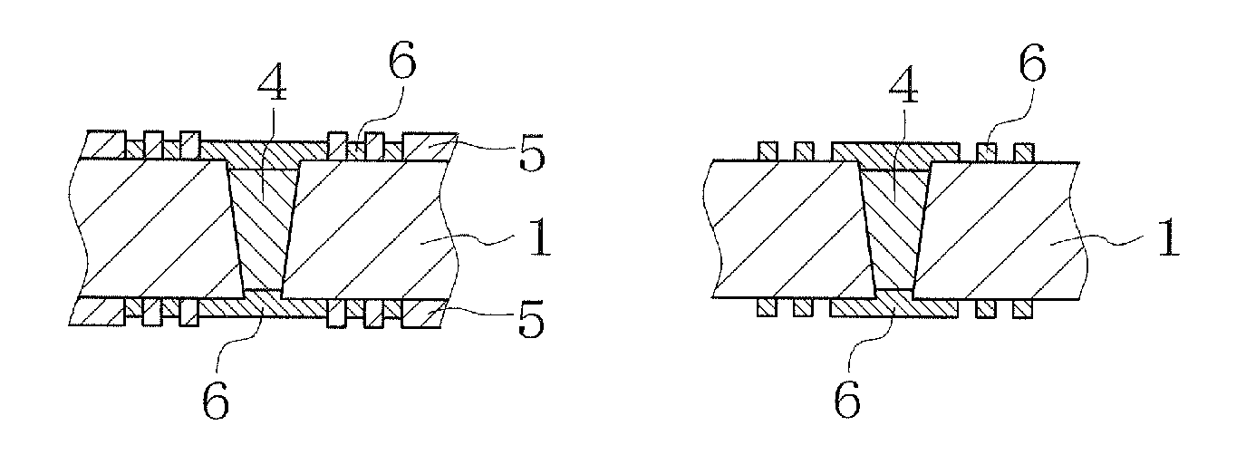
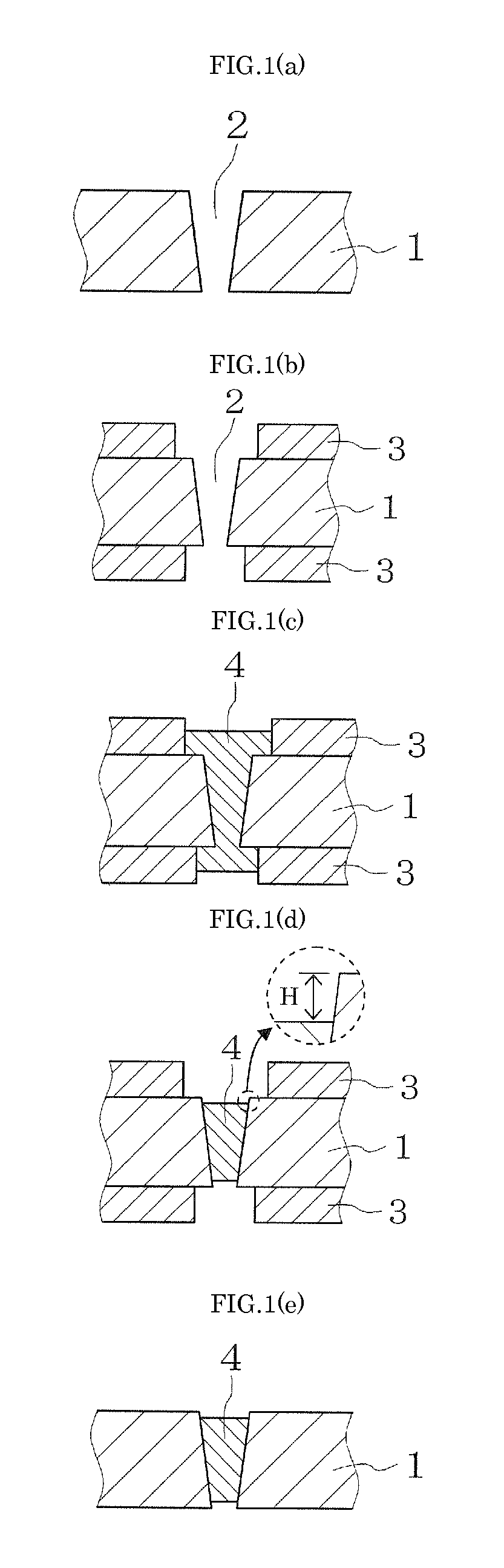
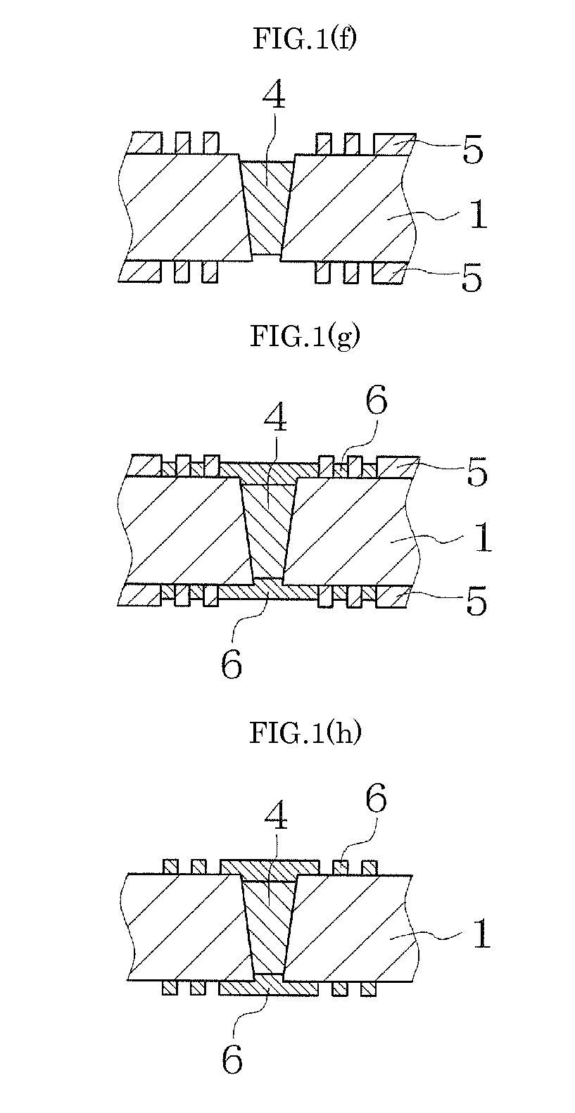
[0011]An example of the embodiment of the present invention is described with reference to FIGS. 1(a) to 1(h). FIGS. 1(a) to 1(h) show a partial cross section of a region that becomes a printed circuit board. The printed circuit board is actually manufactured by means of multi-production printed circuit boards in which a large number of the regions that become the printed circuit boards are arranged longitudinally and laterally on a large board, and discarding allowance regions are disposed therearound.

[0012]Firstly, as shown in FIG. 1(a), the through hole 2 is formed in the insulating layer 1 having an upper surface and a lower surface so as to extend from the upper surface to the lower surface.

[0013]The insulating layer 1 is composed of, for example, an electrical insulation material in which thermosetting resins, such as epoxy resin and bismaleimide-triazine resin, are impregnated in a glass fiber cloth.

[0014]The thickness of the insulating layer 1 is approximately 150-250 μm.

[00...


PUM

PropertyMeasurementUnit
opening diameteraaaaaaaaaa
arithmetic mean roughnessaaaaaaaaaa

Abstract

A method of manufacturing a printed circuit board includes forming a through hole 2 in an insulating layer 1 having upper and lower faces so as to penetrate between the upper and lower surfaces; allowing a first plated conductor 4 to be deposited at least in the through hole 2 and on the upper and lower surfaces around the through hole; removing the first plated conductor overlying and underlying a periphery of the through hole by etching the first plated conductor 4, while leaving at least the first plated conductor 4 in a mid-portion in a vertical direction within the through hole 2; and forming by semi-additive method a second plated conductor 6 that fills an outer portion than the first plated conductor 4 in the through hole 2, and forms a wiring conductor on the upper and lower surfaces.

Description

TECHNICAL FIELD[0001]The present invention relates to a method of manufacturing a printed circuit board.BACKGROUND ART[0002]As a thin type printed circuit board, the printed circuit board as disclosed in, for example, Japanese Unexamined Patent Publication No. 2002-43752 has heretofore been known in which a plurality of tapered through holes are formed in a thin insulating layer, and these through holes are filled with a plated conductor, and wiring conductors formed from the same plated conductor are respectively formed on upper and lower surfaces of the insulating layer.[0003]In this printed circuit board, however, the plated conductor applied to the inside of the through hole, and the wiring conductors formed on the upper and lower surfaces of the insulating layer are formed from the same plated conductor. Therefore, the formation of the plated conductor thick enough to fill these through holes involves the formation of a thick plated conductor having a thickness of approximately...

Claims


Application Information

Patent Timeline
Patent Type & Authority Patents(United States)
IPC IPC(8): H01K3/10
CPCH05K3/426H05K3/427H05K2201/0347H05K2201/09563Y10T29/49117Y10T29/49126Y10T29/49155Y10T29/49165
Inventor OHSUMI, KOHICHIHAYASHI, KAZUNORITSUCHIDA, TOMOHARU
Owner KYOCERA CORP
Why Eureka
Try Eureka