Method of manufacturing glass sheet

a glass sheet and manufacturing method technology, applied in glass making apparatus, manufacturing tools, semiconductor/solid-state device details, etc., can solve the problems of difficult to increase the number of pins, limited mounting space for semiconductor chips to be used in those electronic devices, and high-density mounting of semiconductor chips, etc., to achieve enhanced processing accuracy, high-density wiring, and easy enhancement of processing treatment

Active Publication Date: 2020-08-11
NIPPON ELECTRIC GLASS CO LTD
View PDF18 Cites 0 Cited by
  • Summary
  • Abstract
  • Description
  • Claims
  • Application Information

AI Technical Summary

Benefits of technology

[0007]In order to suppress a change in dimension of a substrate to be processed, it is effective to use a glass sheet as a supporting plate. The glass sheet is smoothened easily on the surface thereof and has stiffness. Accordingly, when the glass sheet is used, the substrate to be processed can be supported strongly and accurately. In addition, the glass sheet easily transmits light, for example, UV light. Accordingly, when the glass sheet is used, the substrate to be processed and the glass sheet can be easily fixed onto each other through formation of an adhesive layer or the like. In addition, the substrate to be processed and the glass sheet can also be easily separated from each other through formation of a peeling layer or the like.
[0012]The glass sheet according to the embodiment of the present invention has a total thickness variation of less than 2.0 μm. When the total thickness variation is decreased to less than 2.0 μm, the accuracy of processing treatment can be easily enhanced. In particular, wiring accuracy can be enhanced, and hence high-density wiring can be performed. In addition, the in-plane strength of the glass sheet is improved, and hence the glass sheet and the laminate are less liable to be broken. Further, the number of times of reuse (number of endurable uses) of the glass sheet can be increased.
[0013]In the glass sheet according to the embodiment of the present invention, all or part of the end surface comprises a melt-solidified surface. With this, microcracks present on the end surface are melted to be eliminated, and the end surface is brought into a smooth state. Therefore, the end surface strength of the glass sheet can be significantly increased.
[0016]Thirdly, it is preferred that in the glass sheet according to the embodiment of the present invention, the melt-solidified surface be formed by laser irradiation. With this, a melt-solidified region of the end surface can be easily regulated. Further, the expanding state of the melt-solidified surface can be easily regulated.

Problems solved by technology

Along with this, a mounting space for semiconductor chips to be used in those electronic devices is strictly limited, and there is a problem of high-density mounting of the semiconductor chips.
However, the conventional WLP has problems in that it is difficult to increase the number of pins, and chipping and the like of semiconductor chips are liable to occur because the semiconductor chips are mounted in a state in which the back surfaces thereof are exposed.

Method used


Image

  • Method of manufacturing glass sheet
  • Method of manufacturing glass sheet
  • Method of manufacturing glass sheet

Examples


example 1

[0081]Now, the present invention is described with reference to Examples. However, Examples below are merely examples, and the present invention is by no means limited to the following Examples.

[0082]Glass raw materials were blended so as to comprise as a glass composition, in terms of mass %, 65.2% of SiO2, 8% of Al2O3, 10.5% of B2O3, 11.5% of Na2O, 3.4% of CaO, 1% of ZnO, 0.3% of SnO2, and 0.1% of Sb2O3. After that, the resultant was loaded into a glass melting furnace to be melted at from 1,500° C. to 1,600° C. Then, the molten glass was supplied into an overflow down-draw forming apparatus to be formed to a thickness of 0.7 mm.

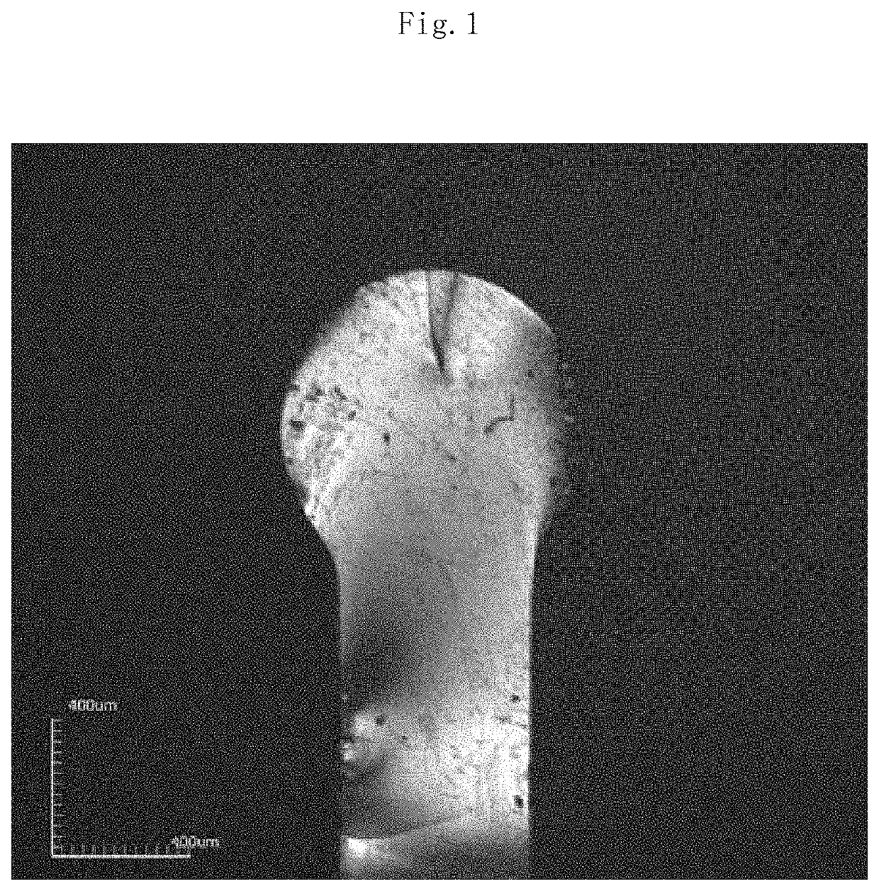
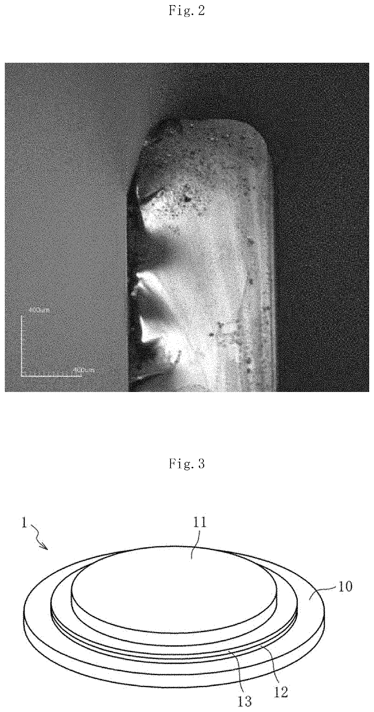
[0083]Next, the obtained mother glass sheet was hollowed out into a wafer shape to provide a glass sheet. The entire end surface of the glass sheet was continuously irradiated with a CO2 laser. Thus, the entire end surface of the glass sheet was melted to form a spherical expanding portion. Then, the resultant was solidified by cooling. Further, the glass ...

example 2

[0091]First, glass raw materials were blended so as to have a glass composition of each of Sample Nos. 1 to 7 shown in Table 4. After that, the resultant was loaded into a glass melting furnace to be melted at from 1,500° C. to 1,600° C. Then, the molten glass was supplied into an overflow down-draw forming apparatus to be formed to a thickness of 0.8 mm. After that, the mother glass sheet was hollowed out into a wafer shape to form a melt-solidified surface on the entire end surface of the obtained glass sheet under the same condition as that of [Example 1], and further subjected to annealing treatment. Each of the obtained glass sheets was evaluated for an average thermal expansion coefficient α30-380 within a temperature range of from 30° C. to 380° C., a density ρ, a strain point Ps, an annealing point Ta, a softening point Ts, a temperature at a viscosity at high temperature of 104.0 dPa·s, a temperature at a viscosity at high temperature of 103.0 dPa·s, a temperature at a visc...


PUM

PropertyMeasurementUnit
thicknessaaaaaaaaaa
thicknessaaaaaaaaaa
thicknessaaaaaaaaaa

Abstract

A technical object of the present invention is to devise a glass sheet that is suitable for supporting a substrate to be processed to be subjected to high-density wiring and has high end surface strength, and a method of manufacturing the glass sheet, to thereby contribute to an increase in density of a semiconductor package. The glass sheet of the present invention has a total thickness variation of less than 2.0 μm, all or part of an end surface of the glass sheet including a melt-solidified surface.

Description

TECHNICAL FIELD[0001]The present invention relates to a glass sheet and a method of manufacturing the glass sheet, and more specifically, to a glass sheet to be used for supporting a substrate to be processed in a manufacturing process for a semiconductor package, and a method of manufacturing the glass sheet.BACKGROUND ART[0002]Portable electronic devices, such as a cellular phone, a notebook-size personal computer, and a personal data assistance (PDA), are required to be downsized and reduced in weight. Along with this, a mounting space for semiconductor chips to be used in those electronic devices is strictly limited, and there is a problem of high-density mounting of the semiconductor chips. In view of this, in recent years, there has been an attempt to perform high-density mounting of a semiconductor package by a three-dimensional mounting technology, that is, by laminating semiconductor chips on top of another and connecting the semiconductor chips through wiring.[0003]In addi...

Claims


Application Information

Patent Timeline
Patent Type & Authority Patents(United States)
IPC IPC(8): C03B29/02C03C19/00H01L23/00C03B33/00C03B17/06C03C3/087C03C3/093C03C3/091C03C23/00C03B33/09H01L21/683H01L21/56
CPCC03C3/093C03C3/091C03C3/087H01L21/6835H01L24/00C03C23/0025C03B17/064C03B29/025H01L24/97C03B29/02C03B33/091H01L24/96C03C19/00H01L21/565H01L2924/3511H01L2224/11002H01L24/11H01L2221/68327H01L2221/68359H01L21/568H01L2224/12105B32B17/06H01L23/15Y02P40/57
Inventor KATAYAMA, HIROKINAKAJIMA
Owner NIPPON ELECTRIC GLASS CO LTD
Why Eureka
Try Eureka