

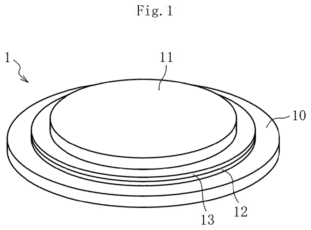
Glass substrate and laminate using same
a technology of glass substrate and laminate, which is applied in the direction of glass forming apparatus, solid-state devices, metal-working apparatus, etc., can solve the problems of difficult to increase the number of pins, limited mounting space for semiconductor chips to be used in those electronic devices, and high-density mounting of semiconductor chips, so as to achieve strong and accurate support of substrates, increase the stiffness of the whole of laminates, and suppress the effect of warping deformation
- Summary
- Abstract
- Description
- Claims
- Application Information
AI Technical Summary
Benefits of technology
Problems solved by technology
Method used
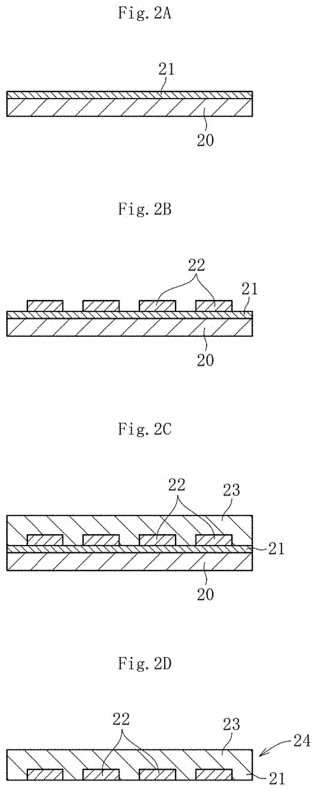
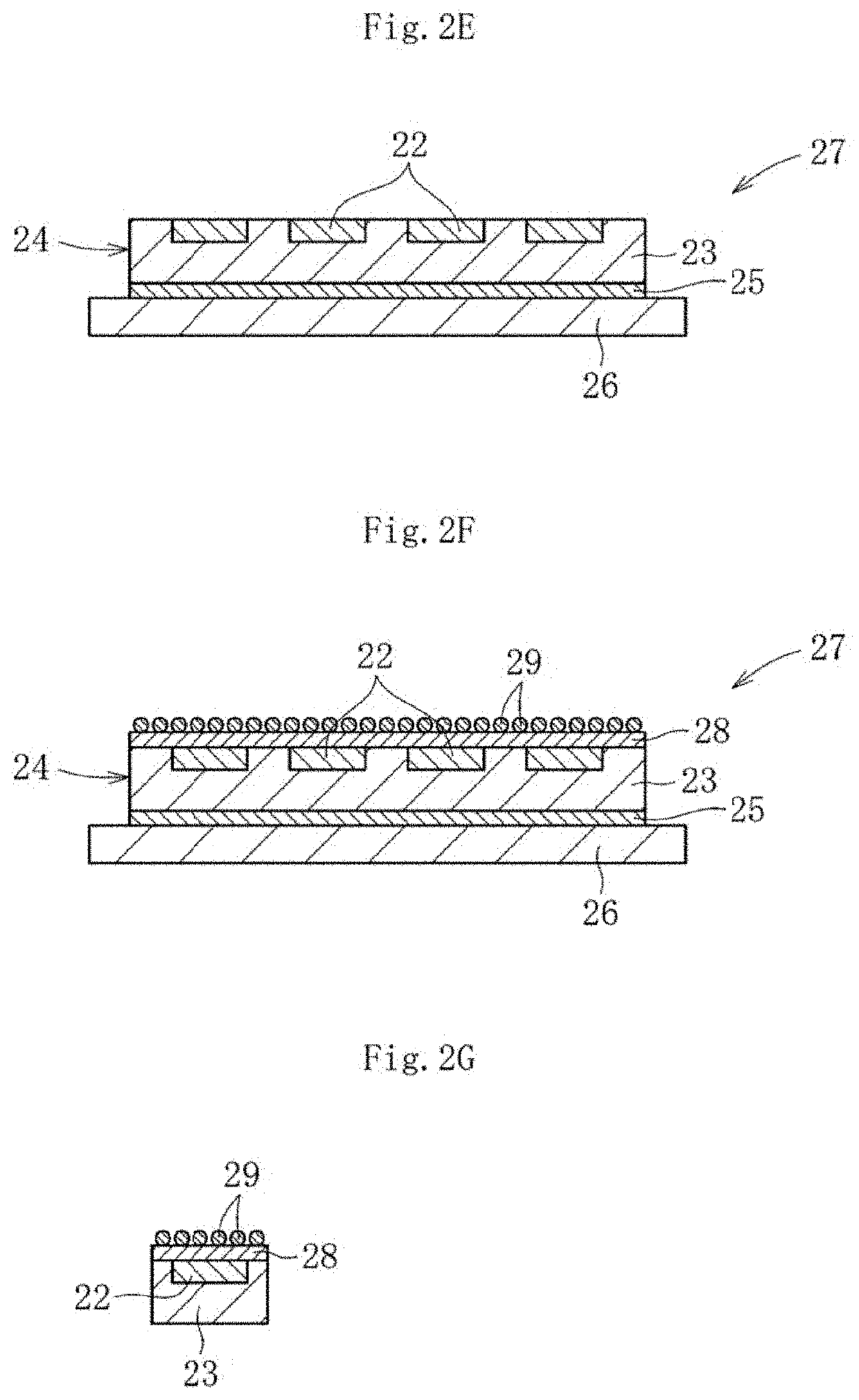
Image

Examples
example 1
[0082]Now, the present invention is described with reference to Examples. However, Examples below are merely examples, and the present invention is by no means limited to the following Examples.
[0083]Glass raw materials were blended so as to comprise as a glass composition, in terms of mass %, 65.2% of SiO2, 8% of Al2O3, 10.5% of B2O3, 11.5% of Na2O, 3.4% of CaO, 1% of ZnO, 0.3% of SnO2, and 0.1% of Sb2O3. After that, the resultant was loaded into a glass melting furnace to be melted at from 1,500° C. to 1,600° C. Then, the molten glass was supplied into an overflow down-draw forming apparatus to be formed to a thickness of 0.7 mm.
[0084]Next, the obtained mother glass sheet was hollowed out into a wafer shape to provide a glass substrate, and the surface of the glass substrate was subjected to polishing treatment with a polishing apparatus to reduce the total thickness variation of the glass substrate. Specifically, both surfaces of the glass substrate were sandwiched between a pair...
example 2
[0087]First, glass raw materials were blended so as to have
[0088]a glass composition of each of Sample Nos. 1 to 7 shown in Table 1. After that, the resultant was loaded into a glass melting furnace to be melted at from 1,500° C. to 1,600° C. Then, the molten glass was supplied into an overflow down-draw forming apparatus to be formed to a thickness of 0.8 mm. Next, under the same conditions as those of [Example 1], the mother glass sheet was hollowed out into a wafer shape, and then, the surface of the obtained glass substrate was subjected to polishing treatment with a polishing apparatus to reduce the total thickness variation of the glass substrate. Further, an information identification part was formed on the glass substrate with a semiconductor laser. Each of the obtained glass substrates was evaluated for an average thermal expansion coefficient α30-380 within a temperature range of from 30° C. to 380° C., a density ρ, a strain point Ps, an annealing point Ta, a softening poi...
PUM
| Property | Measurement | Unit |
|---|---|---|
| thickness | aaaaa | aaaaa |
| distance | aaaaa | aaaaa |
| diameter | aaaaa | aaaaa |
Abstract
Description
Claims
Application Information