Glass sheet

a technology of glass sheet and glass plate, applied in the field of glass sheet, can solve the problems of difficult to increase the number of pins, and the like of semiconductor chips, and achieve the effect of reducing the change in the dimension of the substrate, facilitating light transmission, and strong and accurate suppor

Active Publication Date: 2019-10-15
NIPPON ELECTRIC GLASS CO LTD
View PDF11 Cites 2 Cited by
  • Summary
  • Abstract
  • Description
  • Claims
  • Application Information

AI Technical Summary

Benefits of technology

[0007]In order to suppress a change in dimension of a substrate to be processed, it is effective to use a glass sheet as a supporting sheet. The glass sheet is smoothened easily on the surface thereof and has stiffness. Accordingly, when the glass sheet is used, the substrate to toe processed can be supported strongly and accurately. In addition, the glass sheet easily transmits light, for example, UV light. Accordingly, when the glass sheet is used, the substrate to be processed and the glass sheet can be easily fixed onto each other through formation of an adhesive layer or the like. In addition, the substrate to be processed and the glass sheet can also be easily separated from each other through formation of a peeling layer or the like.
[0012]The glass sheet according to the embodiment of the present invention comprises the position alignment portion. With this, the position of the glass sheet can be easily fixed by bringing a positioning member, for example, a positioning pin, into abutment on the position alignment portion of the glass sheet. As a result, position alignment of the glass sheet and the substrate to be processed is facilitated. Particularly when a position alignment portion is also formed in the substrate to be processed and a positioning member is brought into abutment thereon, the position alignment of the glass sheet and the substrate to be processed is further facilitated.
[0013]However, when the positioning member is brought into abutment on the position alignment portion, of the glass sheet, stress is to be concentrated in the position alignment portion, and hence the glass sheet is liable to be broken with the position alignment portion serving as an origin. Particularly when the glass sheet is curved by an external force, such tendency becomes remarkable. In view of the foregoing, in the glass sheet according to the embodiment of the present invention, all or part of the end edge region of the position alignment portion where the surface thereof and the end surface thereof intersect is chamfered. With this, breakage with the position alignment portion serving as an origin can be effectively avoided. When the position alignment portion is formed in the glass sheet, stress is concentrated in the position alignment portion. Accordingly, stress is less liable to be concentrated in the contour portion occupying a contour region except for the position alignment portion, and hence breakage with the contour portion serving as an origin cart be effectively avoided.
[0025]Ninthly, it is preferred that the glass sheet according to the embodiment of the present invention have a total thickness variation of less than 2.0 μm. When the total thickness variation is decreased, the accuracy of processing treatment can be easily enhanced. In particular, wiring accuracy can be enhanced, and hence high-density wiring can be performed. In addition, the in-plane strength of the glass sheet is improved, and hence the glass sheet and the laminate are less liable to be broken. Further, the number of times of reuse (number of endurable uses) of the glass sheet can be increased. Herein, the “total thickness variation” is a difference between the maximum thickness and the minimum thickness of the entire glass sheet, and may be measured with, for example, SBW-331ML / d manufactured by Kobelco Research Institute, Inc.
[0029]FIG. 4 is a schematic perspective view for illustrating an example of a state in which the position of a laminate 31 according to one embodiment of the present invention is fixed with positioning members 32. In FIG. 4, the laminate 31 comprises a substrate 35 to be processes and a glass sheet 36 configured to support the substrate 35 to be processed. The substrate 35 to be processed and the glass sheet 36 are bonded onto each other in order to prevent a change in dimension of the substrate 35 to be processed. The substrate 35 to be processed comprises a position alignment portion 37, and the glass sheet 36 also comprises a position alignment portion 38. The positioning member 32 is brought into abutment on the position alignment portion 37 of the substrate 35 to be processed and the position alignment portion 38 of the glass sheet 36. Thus, position alignment of the substrate 35 to be processed and the glass sheet 36 is performed. In addition, the positioning members 33, 34 are brought into abutment on a contour portion 39 of the substrate 35 to be processed and a contour portion 40 of the glass sheet 36. In addition, the positions of the substrate 35 to be processed and the glass sheet 36 are fixed with the positioning members 33, 34. Between substrate 35 to be processed and the glass sheet 36, a peeling layer and an adhesive layer (not shown) are arranged. The adhesive layer is brought into contact with the substrate 35 to be processed, and the peeling layer is brought into contact with the glass sheet 36. In FIG. 4, the position alignment portion 37 of the substrate 35 to be processed and the position alignment portion 38 of the glass sheet 36 are brought into abutment on the positioning member 32, but a position alignment portion, may be formed in each of regions to be brought into abutment on the positioning members 33, 34. In this case, the position alignment of the substrate 35 to be processed and the glass sheet 36 can be reliably performed.

Problems solved by technology

Alone with this, a mounting space for semiconductor chips to be used in those electronic devices is strictly limited, and there is a problem of high-density mounting of the semiconductor chips.
However, the conventional WLP has problems in that it is difficult to increase the number of pins, and chipping and the like of semiconductor chips are liable to occur because the semiconductor chips are mounted in a state in which the back surfaces thereof are exposed.
Those steps involve heat treatment at from about 200° C. to about 300° C., and hence there is a risk in that the sealing material may be deformed, and the substrate to be processed may change in dimension.
When the substrate to be processed changes in dimension, it becomes difficult to arrange wiring at high density on one surface of the substrate to be processed, and it is also difficult to form the solder bumps accurately.

Method used


Image

  • Glass sheet
  • Glass sheet
  • Glass sheet

Examples


example 1

[0099]Now, the present invention is described with reference to Examples. However, Examples below are merely examples, and the present invention is by no means limited to the following Examples.

[0100]Glass raw materials were blended so as to comprise as a glass composition, in terms of mass %, 65.5% of SiO2, 8% of Al2O3, 9% of B2O3, 13.1% of Na2O, 3% of CaO, 1% of ZnO, 0.3% of SnO2, and 0.1% of Sb2O3. After that, the resultant was loaded into a glass melting furnace to be melted at from 1,500° C. to 1,600° C. Then, the molten glass, was supplied into an overflow down-draw forming apparatus to be formed to a thickness of 1.0 mm. Further, the resultant was cut to a predetermined size and subjected to annealing treatment.

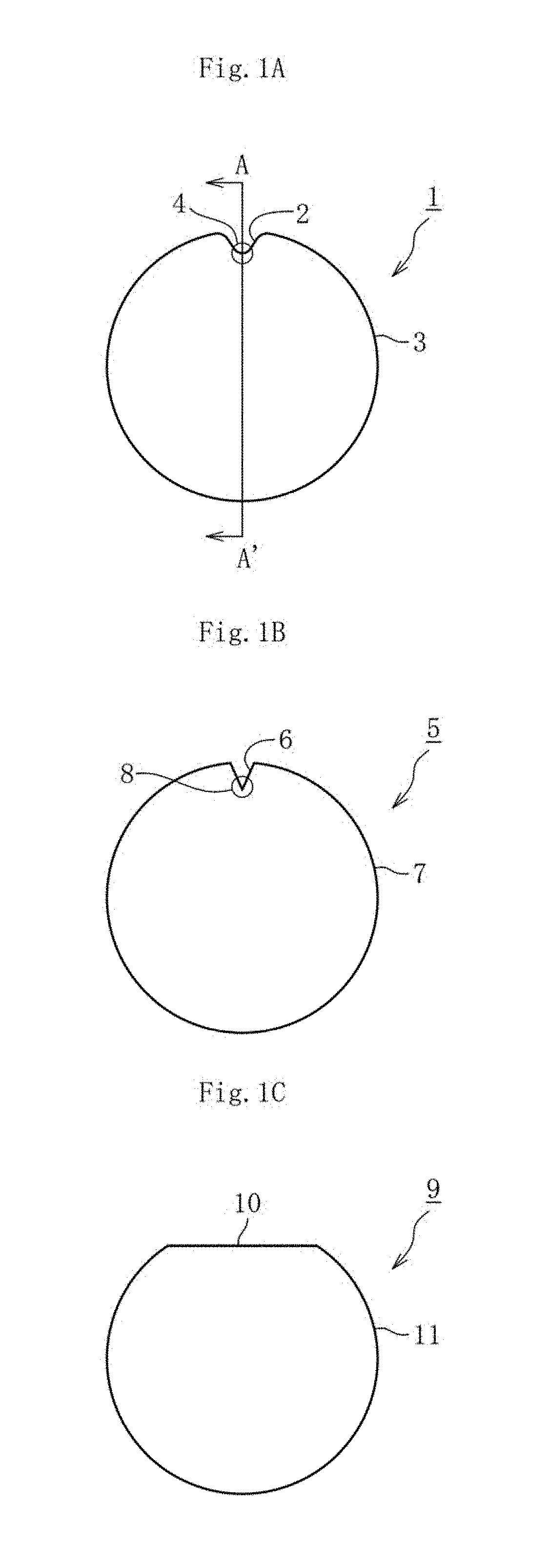
[0101]Next, the outer periphery of the obtained glass sheet was processed into a perfectly circular shape of σ 300 mm. After that, a semicircular recess, that is, a position alignment portion having a notch shape (depth: 1.1 mm) was formed, and the position alignment p...

example 2

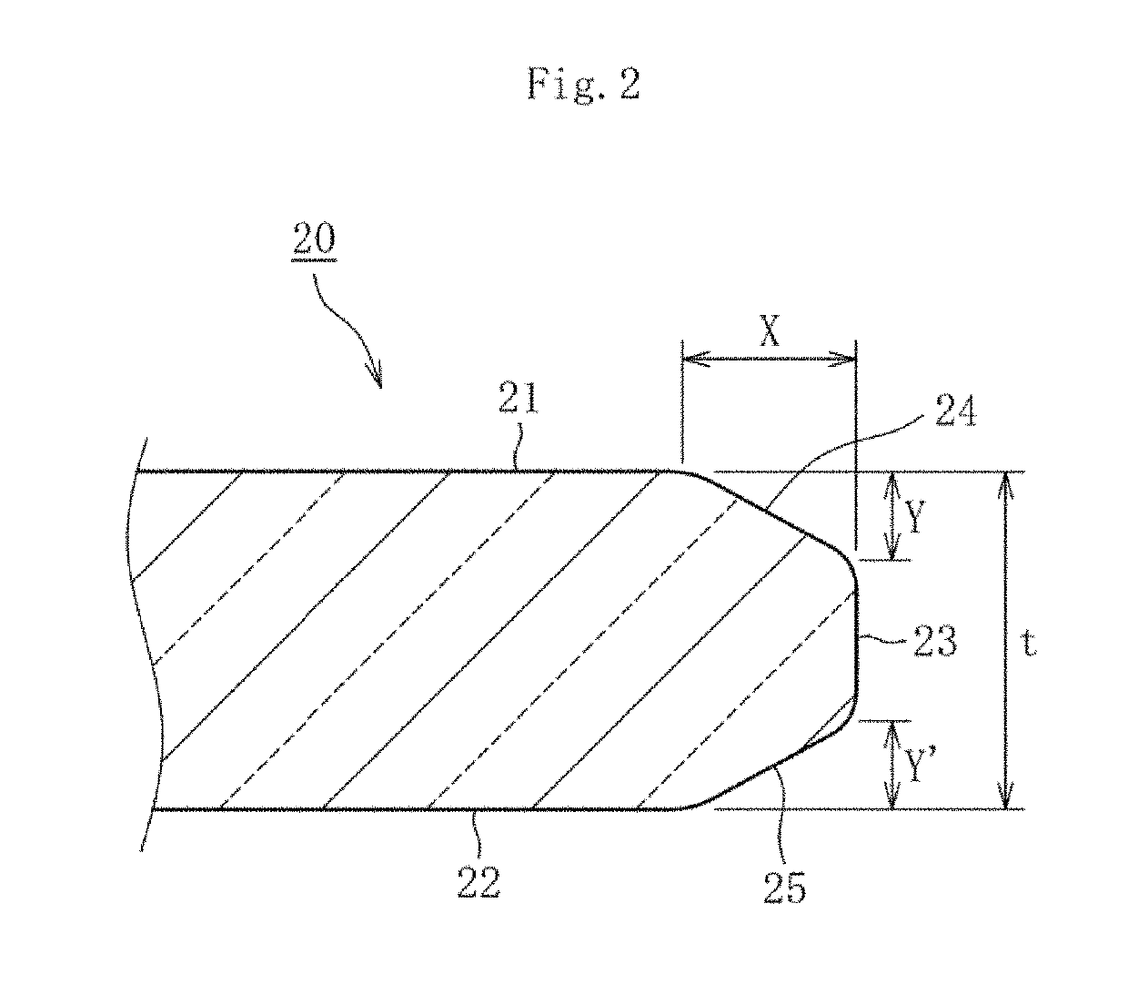
[0106]First, glass raw materials were blended so as to have a glass composition of each of Sample Nos. 1 to 7 shown in Table 2. After that, the resultant was loaded into a glass melting furnace to be melted at from 1,500° C. to 1,600° C. Then, the molten glass was supplied into an overflow down-draw forming apparatus to be formed to a thickness of 0.8 mm. After that, in the same manner as in [Example 1], outer periphery processing was performed, and a position alignment portion having a semicircular recess was formed. Next, the position alignment portion and the contour portion were subjected to chamfering processing. In the chamfering processing, a chamfer width in a thickness direction was set to 50% of a thickness, and a chamfer width in a surface direction was set to 600 μm. In addition, a boundary between the position alignment portion and the contour portion of the glass sheet was processed into a continuously rounded state. Polishing pads used in the chamfering processing are...

example 3

[0115]For each of the position alignment portion and the region except for the position alignment portion (contour portion) of the glass sheet according to Sample No. 2 obtained in [Example 1], the entire end surface including the chamfered surface was subjected to mirror surface polishing treatment, and then the surface of the glass sheet was subjected to polishing treatment with a polishing apparatus by the same method as that of [Example-1]. Polishing pads used in the mirror surface polishing treatment are made of urethane, and the surface subjected to the mirror surface polishing treatment has a polishing roughness of #3000. For comparison, there was also produced a glass sheet in which the entire end surface including the chamfered surface was subjected to polishing treatment with #1500 polishing pads.

[0116]Subsequently, for each of the obtained glass sheets, the surface roughness of the end surface including the chamfered surface was measured by a method in accordance with JIS...


PUM

PropertyMeasurementUnit
surface roughness Raaaaaaaaaaa
widthaaaaaaaaaa
surface roughness Raaaaaaaaaaa

Abstract

A technical object of the present invention is to devise a glass sheet that facilitates position alignment with a substrate to be processed and is less liable to be broken during conveyance, or processing treatment of the substrate to be processed, to thereby contribute to an increase in density of a semiconductor package. In order to achieve the technical object, the glass sheet of the present invention includes, in a contour thereof: a contour portion; and a position alignment portion, in which all or part of an end edge region of the position alignment portion where a surface thereof and an end surface thereof intersect is chamfered.

Description

TECHNICAL FIELD[0001]The present invention relates to a glass sheet, and more specifically, to a glass sheet to be used for supporting a substrate to fee processed in a manufacturing process for a semiconductor package.BACKGROUND ART[0002]Portable electronic devices, such as a cellular phone, a notebook-size personal computer, and a personal data assistance (PDA), are required to be downsized and reduced in weight. Alone with this, a mounting space for semiconductor chips to be used in those electronic devices is strictly limited, and there is a problem of high-density mounting of the semiconductor chips. In view of this, in recent years, there has been an attempt to perform high-density mounting of a semiconductor package by a three-dimensional mounting technology, that is, by laminating semiconductor chips on top of another and connecting the semiconductor chips through wiring.[0003]In addition, a conventional wafer level package (WLP) is manufactured by forming bumps into a wafer...

Claims


Application Information

Patent Timeline
Patent Type & Authority Patents(United States)
IPC IPC(8): C03C19/00H01L21/56H01L21/683C03C3/093C03C3/091B32B7/06B32B7/12B32B17/06H01L23/31H01L23/00C03B17/06
CPCB32B7/06B32B7/12B32B17/06C03C3/091C03C3/093H01L23/3128H01L21/561H01L21/568H01L21/6835H01L2221/68318H01L2224/04105H01L2224/12105H01L2224/96C03B17/064H01L24/96H01L2224/11H01L2224/03B32B17/00C03C19/00H01L23/15Y02P40/57B32B2457/14Y02P40/50H01L2224/95001
Inventor KATAYAMA, HIROKINAKAJIMA
Owner NIPPON ELECTRIC GLASS CO LTD
Why Eureka
Try Eureka