Wiring board having via and method forming a via in a wiring board

a wiring board and via technology, applied in the field of wiring boards, can solve the problems of increasing the influence of noise signals occurring between adjacent lines, reducing the electromagnetic coupling intensity of differential signals transmitted through differential lines, and difficult to ensure signal integrity, so as to reduce the space between vias

Inactive Publication Date: 2013-12-10
NEC CORP
View PDF32 Cites 13 Cited by
  • Summary
  • Abstract
  • Description
  • Claims
  • Application Information

AI Technical Summary

Benefits of technology

[0011]The present invention seeks to solve one or more of the above problems, or to improve upon those problems at least in part. An example of the object is to reduce the space between vias formed in a wiring board.
[0015]According to these inventions, the space between vias formed in a wiring board can be reduced.

Problems solved by technology

As miniaturization of wiring patterns formed on wiring boards advances, and the rate of signal transmission increases, the influence of noise signals occurring between adjacent lines increases.
When the space between the vias is large, there is a problem in which the electromagnetic coupling intensity of the differential signals transmitted through the differential lines will decrease, and in which it will be difficult to ensure signal integrity.
In addition, when the space between the vias is large, there is a problem that the region in which the wiring pattern is to be formed (referred to simply as a wiring region, hereinafter) increases.

Method used


Image

  • Wiring board having via and method forming a via in a wiring board
  • Wiring board having via and method forming a via in a wiring board
  • Wiring board having via and method forming a via in a wiring board

Examples


first exemplary embodiment

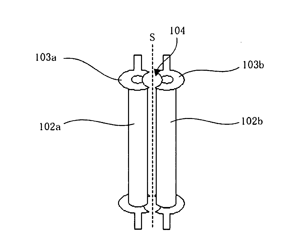
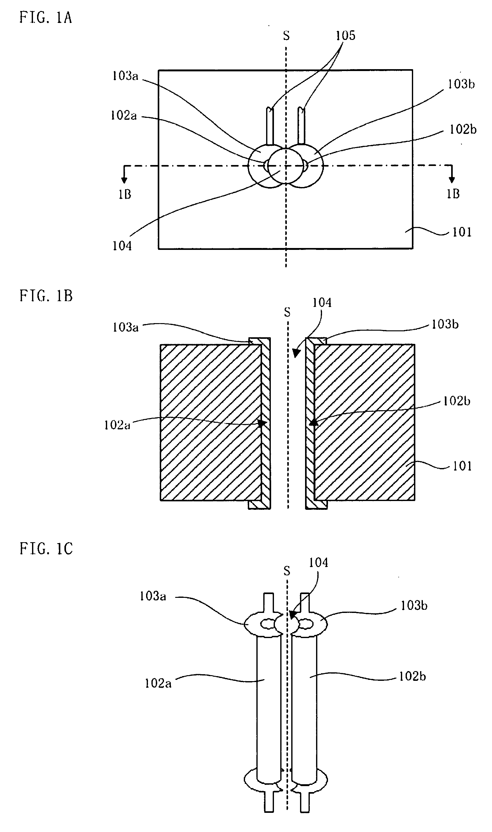
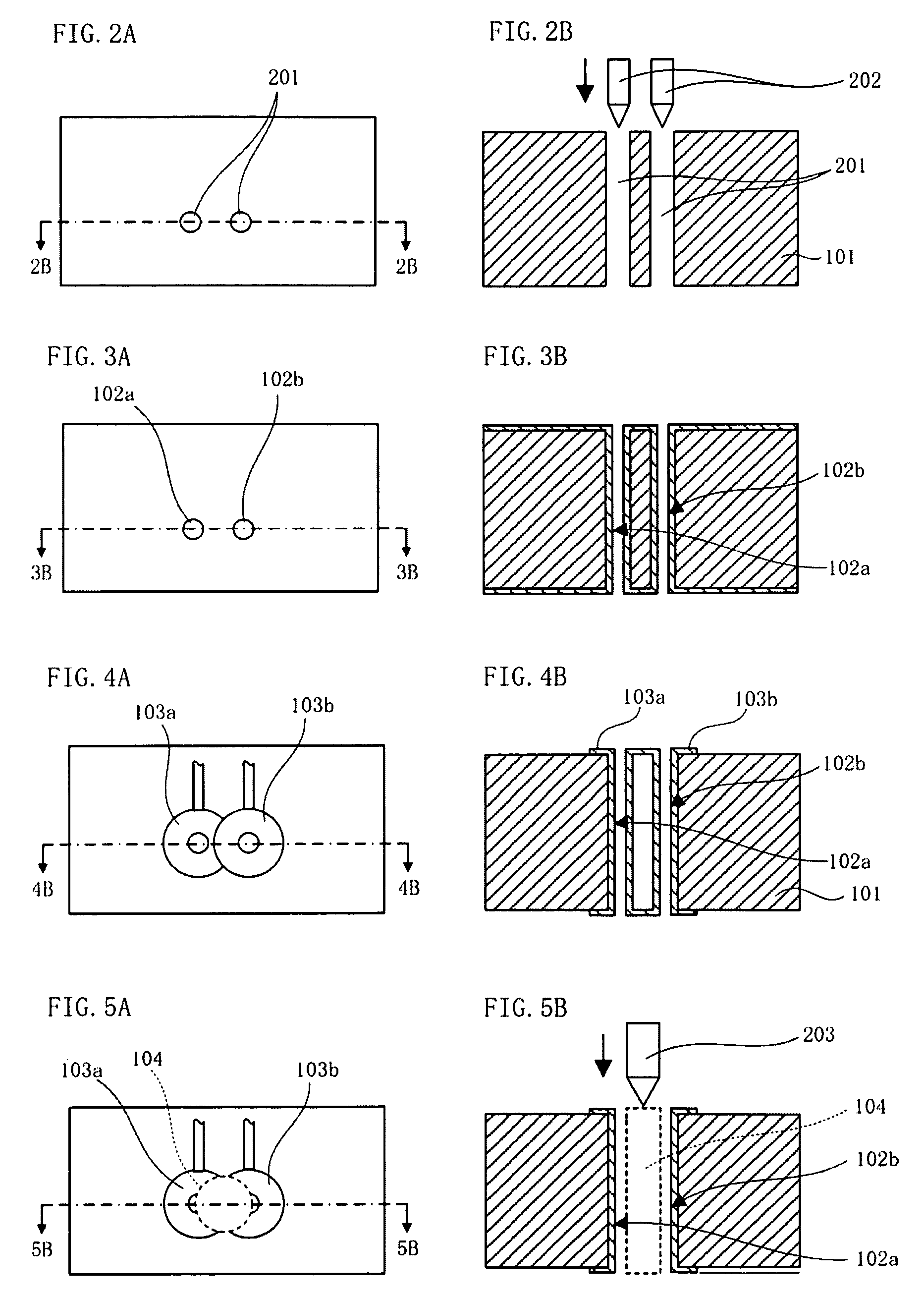
[0036]FIG. 1A is a schematic plan view of a wiring board according to a first exemplary embodiment, and FIG. 1B is a schematic cross-sectional view of the wiring board taken along the line 1B-1B in FIG. 1A. FIG. 1C is a schematic perspective view of lands formed on and vias formed in the wiring board. However, for the sake of clarity, the wiring board is not shown in FIG. 1C.

[0037]Wiring board 101 according to this exemplary embodiment has two wiring layers on which wiring pattern 105 is formed. In addition, first via 102a and second via 102b that electrically connect one of the two wiring layers to another are formed in wiring board 101. First via 102a and second via 102b each comprise a hole that interconnects the wiring layers and a conductor that is formed on the inner surface of the hole. The hole can be partially or completely filled with the conductor.

[0038]On at least one surface of wiring board 101, first land 103a and second land 103b are formed. First land 103a and second...

second exemplary embodiment

[0066]FIG. 6A is a schematic plan view of a wiring board according to a second exemplary embodiment, FIG. 6B is a schematic cross-sectional view of the wiring board taken along the line 6B-6B in FIG. 6A. FIG. 6C is a schematic perspective view of vias formed in and lands formed on the wiring board. However, for the sake of clarity, wiring board 101 is not shown in FIG. 6C.

[0067]Wiring board 101 according to the second exemplary embodiment has four wiring layers. Of the two inner wiring layers that are not exposed on the surfaces of wiring board 101, one wiring layer is grounding (GND) layer 305, and the other wiring layer is power supply layer 304. The two layers exposed on the surfaces of wiring board 101 are signal layers on which wiring pattern 105 for transmitting a signal is formed.

[0068]In this exemplary embodiment, grounding via 302 that electrically connects grounding layer 305 and power supply layer 304 to each other is formed. An insulator is deposited in grounding via 302...

third exemplary embodiment

[0090]According to a third exemplary embodiment, first via 102a and second via 102b penetrate through a wiring board. However, first via 102a and second via 102b electrically connect an outermost layer (a wiring layer exposed on the surface) and an inner wiring layer to each other. That is, first via 102a and second via 102b have stub 401, which is an extra region that does not contribute to signal transmission (see FIG. 10A).

[0091]The presence of such stub 401 causes an increase in capacitance and a mismatch of impedance of wiring board 101. Therefore, stub 401 is preferably removed from wiring board 101.

[0092]In the following, a via forming method that includes a step of removing a stub will be described with reference to FIGS. 10A to 10D.

[0093]FIG. 10A is a schematic cross-sectional view of a wiring board at the time when the first step in the via forming method is completed. Up to the first step, the via forming method is the same as in the first and second exemplary embodiments...


PUM

PropertyMeasurementUnit
frequencyaaaaaaaaaa
signal transmissionaaaaaaaaaa
distanceaaaaaaaaaa

Abstract

A wiring board has a plurality of wiring layers, a first land, a second land, a first via and a second via. The first land and the second land are formed on at least one wiring layer of the wiring board and are disposed to partially overlap with each other. The first via and the second via are formed in association with the first land and the second land, respectively. The first via and the second via electrically connect a first wiring layer and a second wiring layer of the plurality of wiring layers to each other. The wiring board has a separator that is formed by a hole that separates the first land and the second land from each other.

Description

[0001]This application is based upon and claims the benefit of priority from Japanese patent application No. 2008-183665, filed on Jul. 15, 2008, the disclosure of which is incorporated herein in its entirety by reference.BACKGROUND OF THE INVENTION[0002]1. Field of the Invention[0003]The present invention relates to a wiring board having a plurality of wiring layers, method forming a via in the wiring board, and a method of manufacturing the wiring board.[0004]2. Description of the Related Art[0005]As miniaturization of wiring patterns formed on wiring boards advances, and the rate of signal transmission increases, the influence of noise signals occurring between adjacent lines increases. To reduce such noise, a wiring board having a pair of signal lines (referred to as differential lines, hereinafter) for transmitting differential signals has been in practical use.[0006]A wiring board having a plurality of wiring layers has a via formed for electrically connecting the wiring layer...

Claims


Application Information

Patent Timeline
Patent Type & Authority Patents(United States)
IPC IPC(8): H05K3/42H05K1/11H05K3/30
CPCH05K1/115H05K3/429H05K1/0237H05K3/42H05K2201/09627H05K2201/09636H05K2201/09645H05K2201/09809H05K2203/0242H05K2203/175Y10T29/49139Y10T29/49156Y10T29/49135
Inventor TAKEDA, TSUTOMU
Owner NEC CORP
Why Eureka
Try Eureka