Video format conversion without a flicker for the solid imaging apparatus

a solid imaging and video format technology, applied in the field of imaging apparatus, can solve the problem that the 0-degree phase having the maximum amplitude cannot be effectively utilized to reduce the resolution, and achieve the effect of less jitter

Inactive Publication Date: 2013-12-10
KOKUSA ELECTRIC CO LTD
View PDF8 Cites 0 Cited by
  • Summary
  • Abstract
  • Description
  • Claims
  • Application Information

AI Technical Summary

Benefits of technology

[0018]It is an object of the present invention is to output image subjected to scanning line conversion so that there is less jitter than conventional scanning line conversion.
[0022]a method of changing pairs of vertical pixels subjected to vertical pixel addition to odd and even fields to be read out as image signals of interlaced scanning from the CCD, rendering arrangement phase including a greater symmetric such that reducing singular points in correlation of arrangement phases of scanning lines of image signals of the interlaced scanning and arrangement phases of scanning lines of image signals of second progressive scanning, subjecting the image signals to scanning line conversion by additional average of scanning lines of several kinds of coefficients having vertical frequency characteristics approximating to one another to be converted into image signals of second progressive scanning and outputting image signals of second progressive scanning.
[0028]According to the present invention, image subjected to scanning line conversion so that there is less jitter than conventional scanning line conversion can be outputted.

Problems solved by technology

Accordingly, moiré (flicker and jitter in vertical direction) or the like is liable to be caused to degrade the image quality and the conversion characteristic of filter is required to be approximated to 180-degree phase having the least amplitude in order to approximate the conversion characteristic of filter for improvement of the above defects, so that the merit of the 0-degree phase having maximum amplitude cannot be utilized effectively to reduce the resolution.

Method used


Image

  • Video format conversion without a flicker for the solid imaging apparatus
  • Video format conversion without a flicker for the solid imaging apparatus
  • Video format conversion without a flicker for the solid imaging apparatus

Examples


embodiment 1

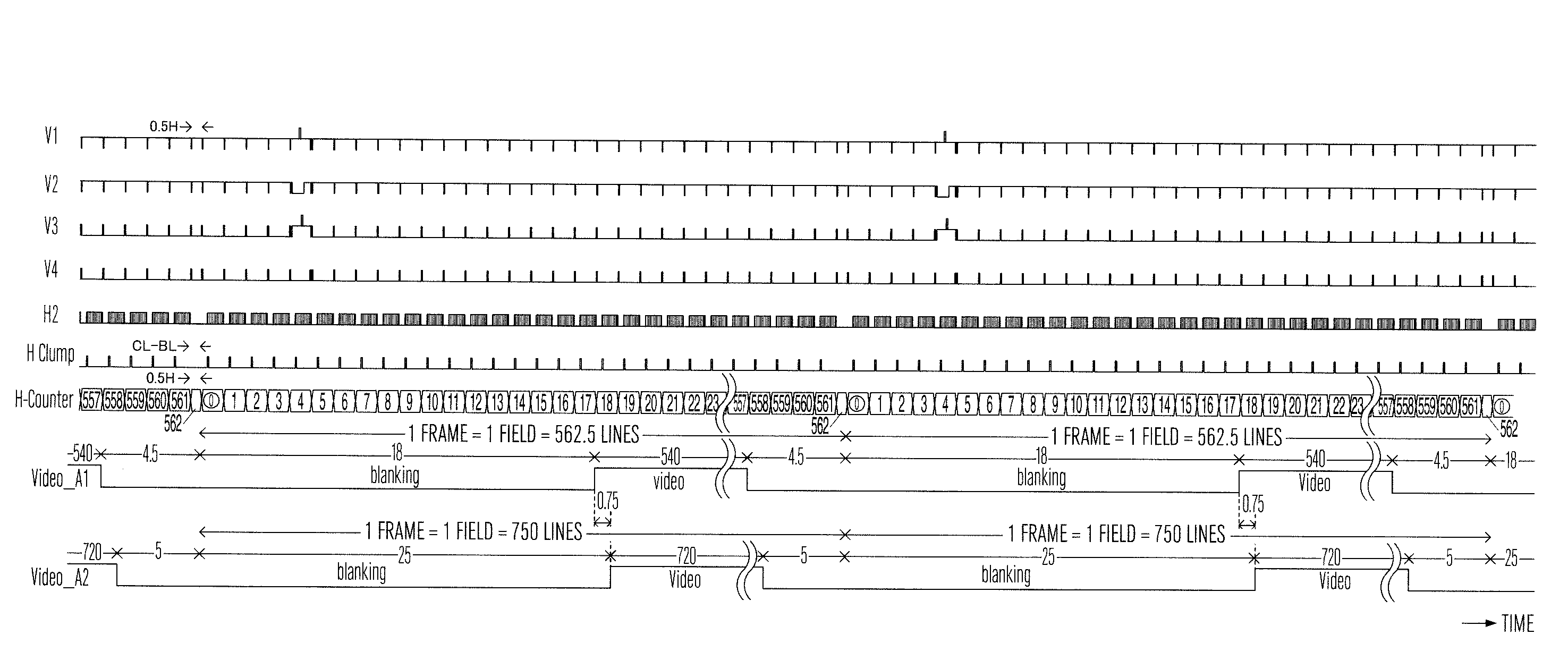
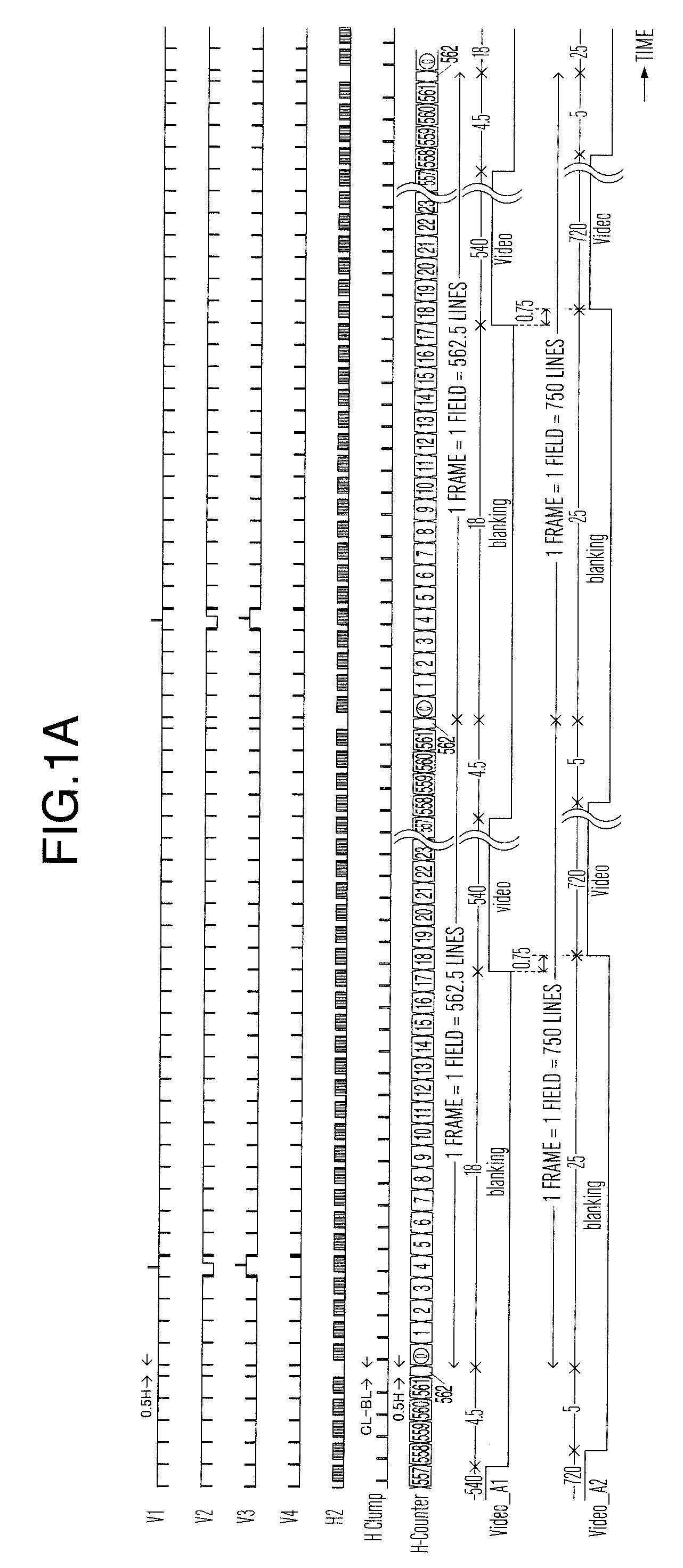
[0072]Referring now to FIG. 1A of a timing chart showing operation an imaging apparatus according to an embodiment of the present invention and FIG. 2 showing a schematic diagram illustrating vertical pixel addition operation of the imaging apparatus of the embodiment of the present invention, the embodiment of the present invention is described.

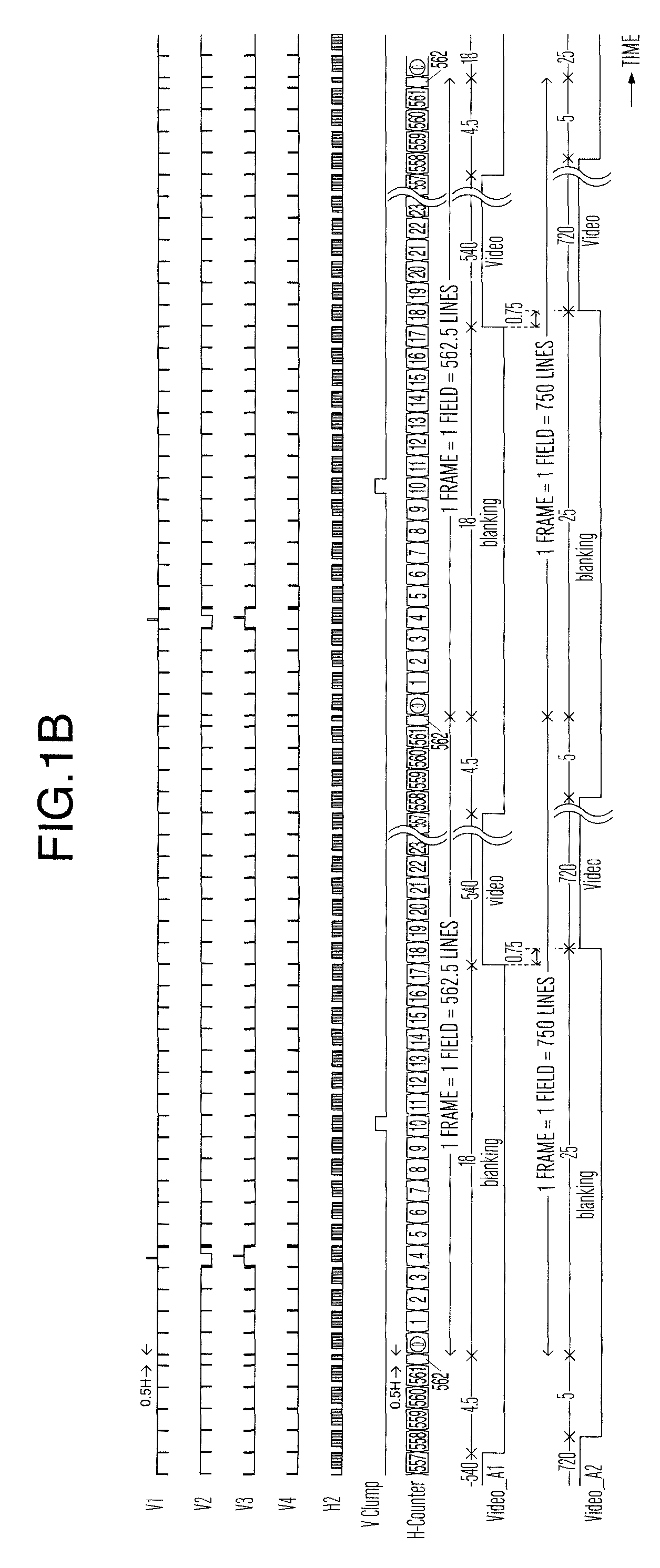
[0073]Referring together to FIG. 1B of a timing chart showing operation of an imaging apparatus according to another embodiment of the present invention, difference of measures different from FIG. 1A is described.

[0074]In FIG. 1A of the timing chart showing operation of the imaging apparatus according to the embodiment of the present invention, V1-V4 represent operation of reading vertical transfer of vertical transfer paths V1 to V4 in IT-CCD. Concretely, V1 to V4 represent reading of electric charges from PD to V1 and V3, vertical pixel addition using V2 and vertical transfer operation for a set of V1 to V4. In the embodiment, description ...

embodiment 2

[0096]Another embodiment of the present invention is now described with reference to FIG. 3 of a timing chart showing operation of an imaging apparatus according to another embodiment of the present invention and FIGS. 4A, 4B, 4C of a schematic diagram illustrating vertical pixel addition operation of the imaging apparatus according to another embodiment of the present invention.

[0097]In FIG. 3 of the timing chart showing operation of the imaging apparatus according to the embodiment of the present invention, V1 to V4 represent operation of reading vertical transfer of vertical transfer paths V1 to V4 in IT-CCD. Concretely, reading of electric charges from PD to V1 and V3, vertical pixel addition of odd field image using V2 and vertical pixel addition of even field image using V4 and vertical transfer operation for a set of V1 to V4 are shown.

[0098]In FIG. 3, the periods of odd field and even field are different by 1H from each other.

[0099]In FIG. 3, H2 represents operation of horiz...


PUM


Abstract

In an imaging apparatus which subjects signal electric charges of photodiodes of IT-CCD for interlaced scanning of 1080 effective scanning lines to vertical pixel addition to be read out as image signals, at least one of vertical transfer at the last horizontal period and horizontal transfer at half period in reading of pixels is stopped while fixing pairs of vertical pixels to be subjected to vertical pixel addition to be read out as image signals of progressive scanning of 540 effective scanning lines from the CCD and the read-out image signals of 540 effective scanning lines are subjected to scanning line conversion of 3 to 4 to be converted into image signals of progressive scanning of 720 effective scanning lines, the image signals of progressive scanning of 720 effective scanning lines being outputted.

Description

INCORPORATION BY REFERENCE[0001]The present application claims priority from Japanese application JP-2010-100916 filed on Apr. 26, 2010, the content of which is hereby incorporated by reference into this application.BACKGROUND OF THE INVENTION[0002]The present invention relates to an imaging apparatus including solid imaging devices.[0003]In imaging devices made of silicon, an electrode voltage such as substrate voltage is varied to change the saturation characteristic of photodiodes (PD). A positive pulse voltage is applied to an overflow drain (OD) of substrate (Sub) to thereby sweep away electric charges of photodiodes. FIT-CCD (Frame Interline Transfer—Charge-Coupled Device) and IT-CCD (Interline Transfer—Charge-Coupled Device) among CCD's (Charge-Coupled Devices) have overflow drain formed by substrate and named vertical-type overflow drain (refer to CCD area image sensor, 39781AE Panasonic Inc.)[0004]FIG. 5B is a block diagram schematically illustrating a conventional imaging ...

Claims


Application Information

Patent Timeline
Patent Type & Authority Patents(United States)
IPC IPC(8): H04N3/14H04N5/335
CPCH04N5/3722H04N25/715
Inventor KOSAKA, HIROKI
Owner KOKUSA ELECTRIC CO LTD
Why Eureka
Try Eureka