Termination control circuit and semiconductor device including the same

a control circuit and semiconductor technology, applied in the direction of digital storage, instruments, and increasing the degree of modification, can solve the problems of inability to provide impedance matching, error during signal transmission, and inability to ensure termination operation

Active Publication Date: 2013-12-17
SK HYNIX INC
View PDF3 Cites 1 Cited by
  • Summary
  • Abstract
  • Description
  • Claims
  • Application Information

AI Technical Summary

Problems solved by technology

In this case, when an impedance-matching is not appropriately provided, the transmitted signals may be reflected and thus, errors may occur during signal transmission.
However, when a fixed resistance is applied to the outside, the impedance-matching may not be provided due to aging or temperature change of an integrated circuit or a deviation in a manufacturing process.
However, in the DRAM, the termination operation may not be guaranteed when a delay lock loop (DLL) included in the DRAM is inactivated.
Therefore, when the write operation is performed if the delay lock loop is inactivated, the impedance matching for the termination end may be not provided, thereby causing an error in writing data.

Method used


Image

  • Termination control circuit and semiconductor device including the same
  • Termination control circuit and semiconductor device including the same
  • Termination control circuit and semiconductor device including the same

Examples


Embodiment Construction

[0021]Exemplary embodiments of the present invention will be described below in more detail with reference to the accompanying drawings. The present invention may, however, be embodied in different forms and should not be construed as limited to the embodiments set forth herein. Rather, these embodiments are provided so that this disclosure will be thorough and complete, and will fully convey the scope of the present invention to those skilled in the art. Throughout the disclosure, like reference numerals refer to like parts throughout the various figures and embodiments of the present invention.

[0022]Hereinafter, exemplary embodiments of the present invention will be described with reference to the accompanying drawings so that a person with an ordinary skilled in the art to which the present invention pertains can easily carry out technical ideas of the present invention.

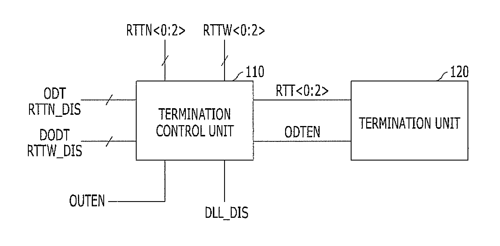
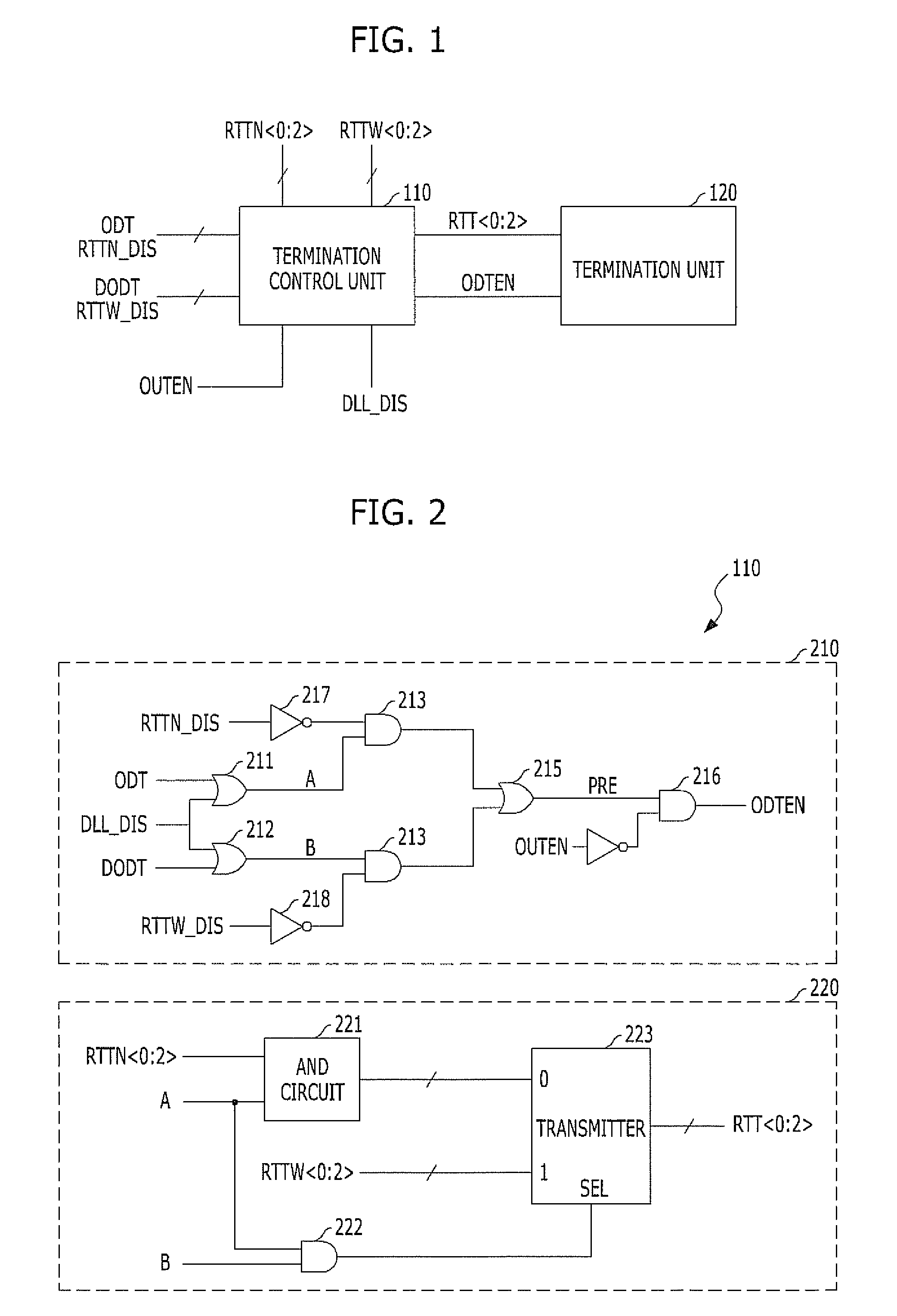
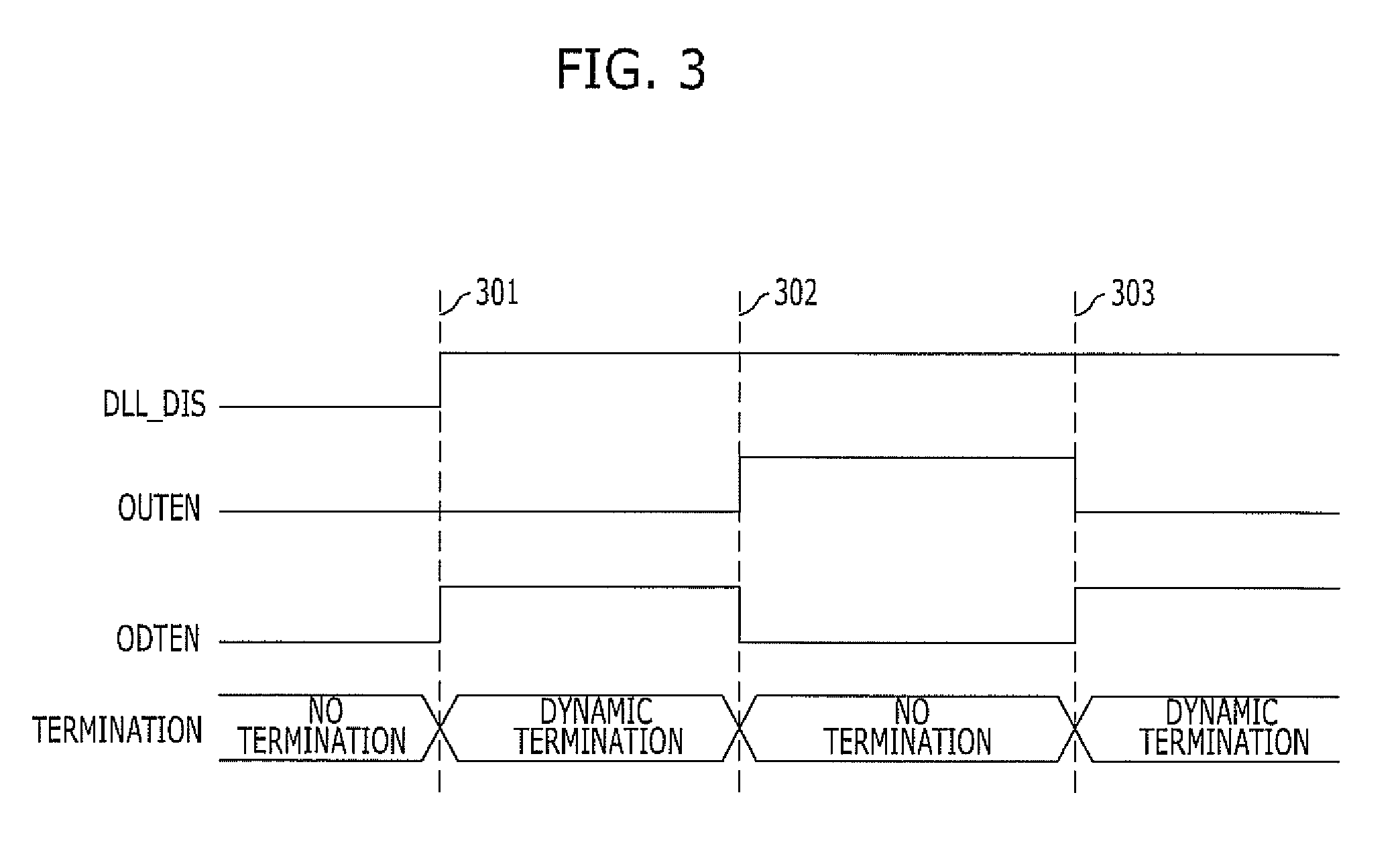
[0023]FIG. 1 is a block diagram of showing a semiconductor device in accordance with an exemplary embodiment of...


PUM


Abstract

The semiconductor device includes a termination control unit configured to generate a termination enable signal and termination resistance information in response to termination activation information, dynamic activation information, normal resistance information, and dynamic resistance information wherein the termination enable signal is activated when a delay lock loop is inactivated, and a termination unit configured to be controlled in response to the termination enable signal and terminate an interface pad by using a resistance value determined by the termination resistance information.

Description

CROSS-REFERENCE TO RELATED APPLICATIONS[0001]The present application claims priority of Korean Patent Application No. 10-2011-0017659, filed on Feb. 28, 2011, which is incorporated herein by reference in its entirety.BACKGROUND[0002]1. Field[0003]Exemplary embodiments of the present invention relate to a semiconductor device and more particularly, a semiconductor device for controlling a dynamic termination operation.[0004]2. Description of the Related Art[0005]As the capacity and speed of a semiconductor memory device, e.g., Dynamic Random Access Memory (DRAM) is increased and a Double Data Rate Static Dynamic Random Access Memory (DDR SDRAM) is widely used, various new concepts for more increasing a transmission rate of a memory device have been introduced. Among those, a resistance of a termination end is typically employed for smoothly transmitting signals among devices.[0006]In this case, when an impedance-matching is not appropriately provided, the transmitted signals may be r...

Claims


Application Information

Patent Timeline
Patent Type & Authority Patents(United States)
IPC IPC(8): H03K19/003
CPCH03K19/0005G11C11/4096G11C11/4093G11C7/10
Inventor JUNG, JONG-HO
Owner SK HYNIX INC
Why Eureka
Try Eureka