Eureka AIR delivers breakthrough ideas for toughest innovation challenges, trusted by R&D personnel around the world.

Method for manufacturing light emitting diodes including forming circuit structures with a connecting section

a technology of light-emitting diodes and connecting sections, which is applied in the direction of semiconductor devices, semiconductor/solid-state device details, electrical apparatus, etc., can solve the problems of low yield rate of leds and waste of processing tim

Active Publication Date: 2014-02-04
ADVANCED OPTOELECTRONICS TECH
View PDF5 Cites 0 Cited by
  • Summary
  • Abstract
  • Description
  • Claims
  • Application Information

AI Technical Summary

Benefits of technology

[0005]In general, the LEDs are formed by dividing an LED wafer. The LED wafer includes a substrate, LED chips arranged on the substrate and an encapsulation covering the LED chips. An upper surface and a bottom surface of the substrate have metal electrodes formed thereon. In manufacture of the LEDs, the metal electrodes have to be etched to insulate from each other. In addition, a plurality of holes are defined in the substrate and filled with electrical conductive materials to electrically connect the metal electrodes on the upper surface and lower surface of the substrate. The process wastes a lot of time and the yielding rate of the LEDs is relatively low.

Problems solved by technology

The process wastes a lot of time and the yielding rate of the LEDs is relatively low.

Method used


Image

  • Method for manufacturing light emitting diodes including forming circuit structures with a connecting section
  • Method for manufacturing light emitting diodes including forming circuit structures with a connecting section
  • Method for manufacturing light emitting diodes including forming circuit structures with a connecting section

Examples


Embodiment Construction

[0016]An embodiment of the present disclosure will now be described in detail below, with reference to the accompanying drawings.

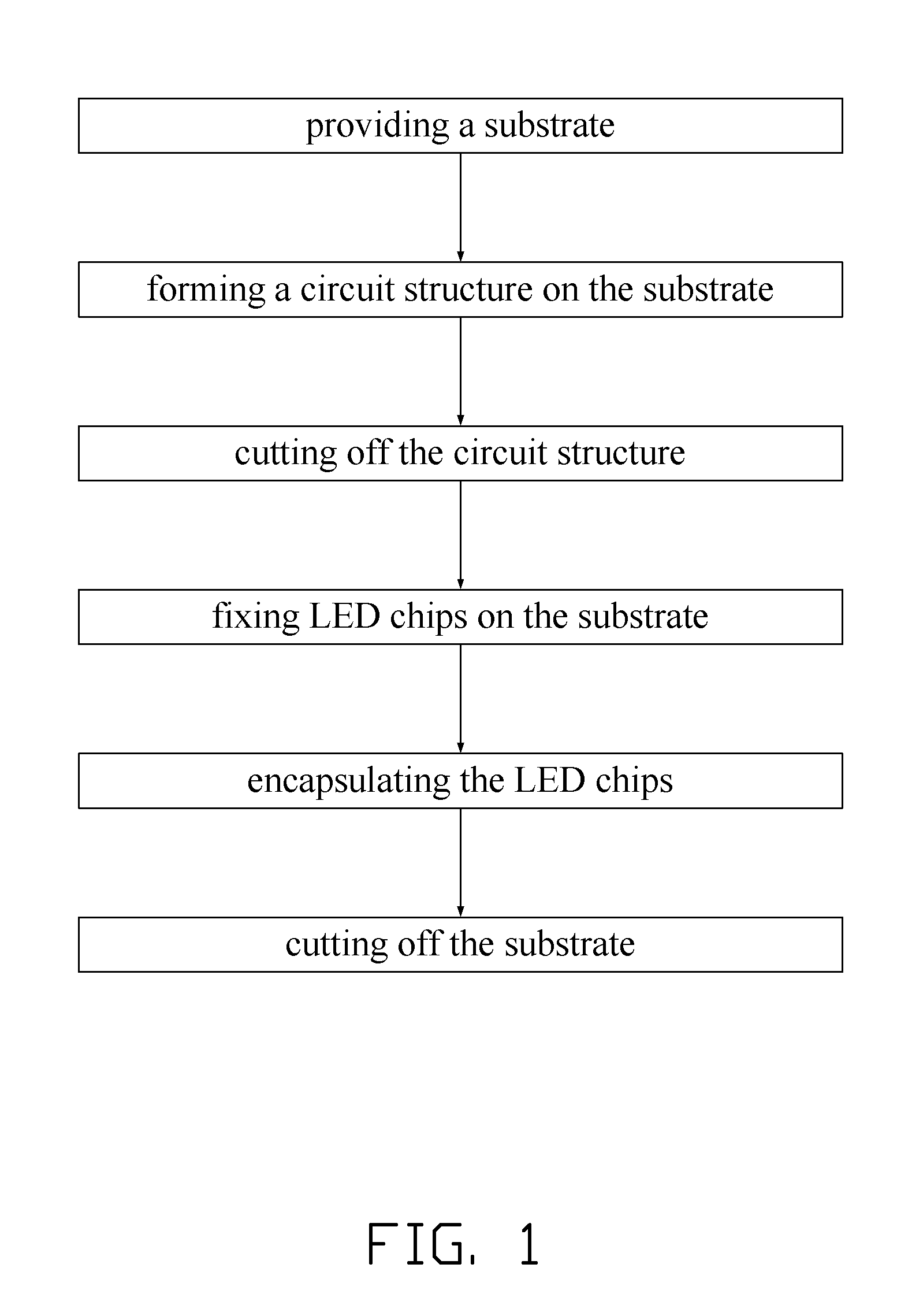
[0017]FIG. 1 shows a flow chart of a method for manufacturing an LED according to an exemplary embodiment of the present disclosure. The method for manufacturing the LED includes following steps: providing a substrate; forming a circuit structure on the substrate; cutting the circuit structure; fixing LED chips on the substrate; encapsulating the LED chips; and cutting the substrate. Details are given below.

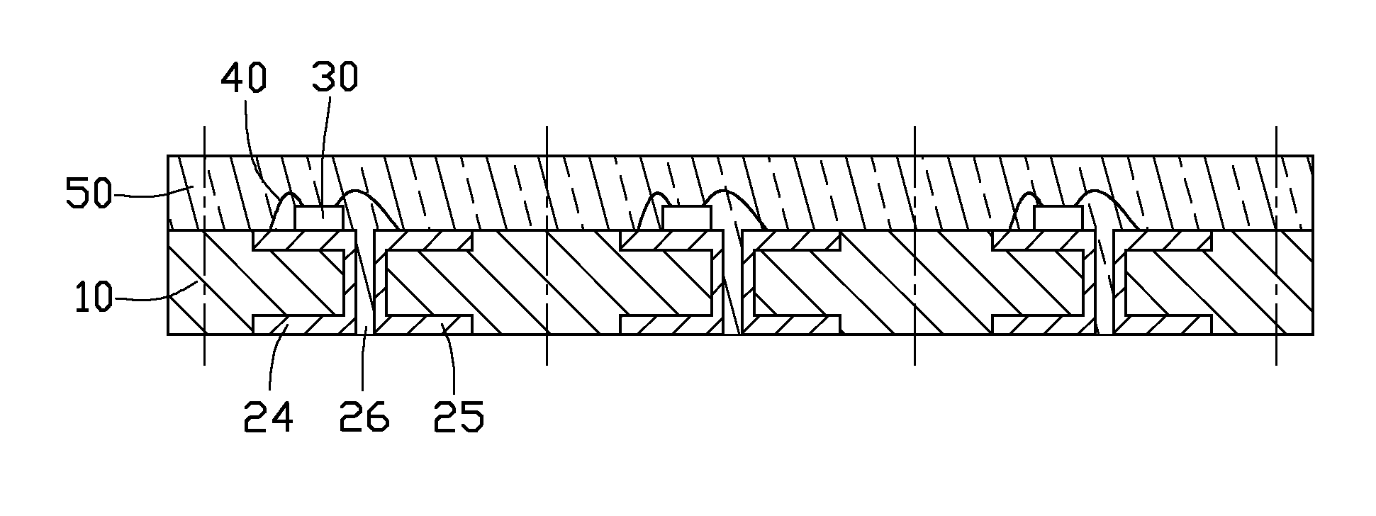
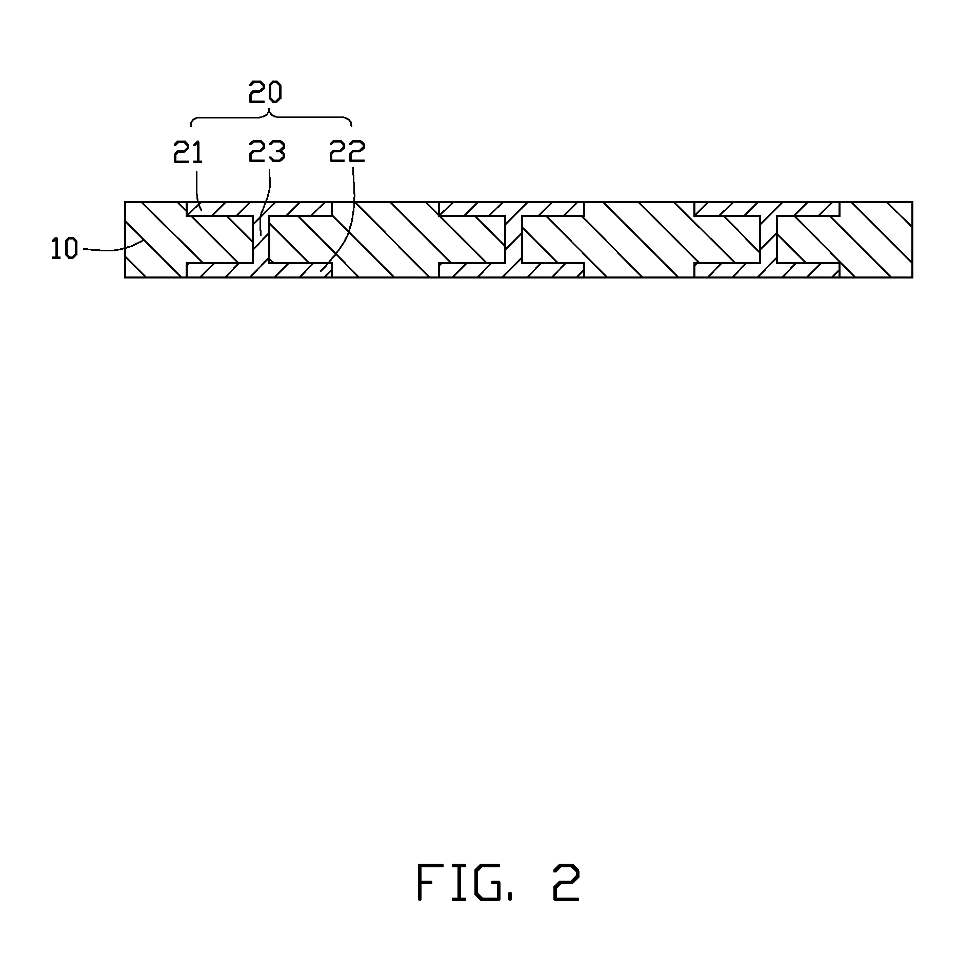
[0018]Referring to FIG. 2, firstly, the substrate 10 is provided. The substrate 10 can be made of a material selected from a group consisting of sapphire, ZnO, silicate, and ceramic. In this embodiment, the substrate 10 has a plurality of concaves respectively formed in an upper surface and a bottom surface thereof. The concaves are in a uniform interval. A plurality of through holes extends through the substrate 10. Each through hole is aligned with an...


PUM


Abstract

A method for manufacturing LEDs includes following steps: forming circuit structures on a substrate, each circuit structure having a first metal layer and a second metal layer formed on opposite surfaces of the substrate and a connecting section interconnecting the first and second metal layers; cutting through each circuit structure along a middle of the connecting section to form first and second electrical connecting portions insulated from each other via a gap therebetween; arranging LED chips on the substrate and electrically connecting the LED chips to the first and second electrical connecting portions; forming an encapsulation on the substrate to cover the LED chips; and cutting through the substrate and the encapsulation between the first and second electrical connecting portions of neighboring circuit structures to obtain the LEDs.

Description

BACKGROUND[0001]1. Technical Field[0002]The present disclosure relates to a method for manufacturing semiconductor lighting devices, and particularly, to a method for manufacturing light emitting diodes. The present disclosure also relates to light emitting diodes obtained by the method.[0003]2. Description of Related Art[0004]Light emitting diodes (LEDs) have many beneficial characteristics, including low electrical power consumption, low heat generation, long lifetime, small volume, good impact resistance, fast response and excellent stability.[0005]In general, the LEDs are formed by dividing an LED wafer. The LED wafer includes a substrate, LED chips arranged on the substrate and an encapsulation covering the LED chips. An upper surface and a bottom surface of the substrate have metal electrodes formed thereon. In manufacture of the LEDs, the metal electrodes have to be etched to insulate from each other. In addition, a plurality of holes are defined in the substrate and filled w...

Claims


Application Information

Patent Timeline
Patent Type & Authority Patents(United States)
IPC IPC(8): H01L33/00H01L23/12H01L23/22H01L23/52H01L23/24H01L21/00
CPCH01L24/97H01L2924/01029H01L2933/0066H01L2924/12041H01L33/62H01L33/52H01L2224/97H01L2924/15787H01L2224/48091H01L2924/00014H01L2224/85H01L2924/00
Inventor CHANG, CHAO-HSIUNG
Owner ADVANCED OPTOELECTRONICS TECH
Why Eureka
Eureka Blog
Learn More