Nonvolatile memory device with a clamping voltage generation circuit for compensating the variations in memory cell parameters

a nonvolatile memory device and clamping voltage generation circuit technology, applied in the field of electronic memory technologies, can solve the problems of degrading other aspects and reducing reliability, and achieve the effect of improving the reliability of read operations

Active Publication Date: 2014-02-18
SAMSUNG ELECTRONICS CO LTD
View PDF8 Cites 22 Cited by
  • Summary
  • Abstract
  • Description
  • Claims
  • Application Information

AI Technical Summary

Benefits of technology

[0008]These and other embodiments of the inventive concept can potentially improve the reliability of read operations performed in nonvolatile memory devices such as MRAMs, for example.

Problems solved by technology

However, as improvements are made to one aspect of a memory device, other aspects may be degraded.
For instance, as operating speed is increased, reliability may decrease.

Method used


Image

  • Nonvolatile memory device with a clamping voltage generation circuit for compensating the variations in memory cell parameters
  • Nonvolatile memory device with a clamping voltage generation circuit for compensating the variations in memory cell parameters
  • Nonvolatile memory device with a clamping voltage generation circuit for compensating the variations in memory cell parameters

Examples


Embodiment Construction

[0029]Selected embodiments of the inventive concept are described below with reference to the accompanying drawings. These embodiments are presented as teaching examples and should not be construed to limit the scope of the inventive concept.

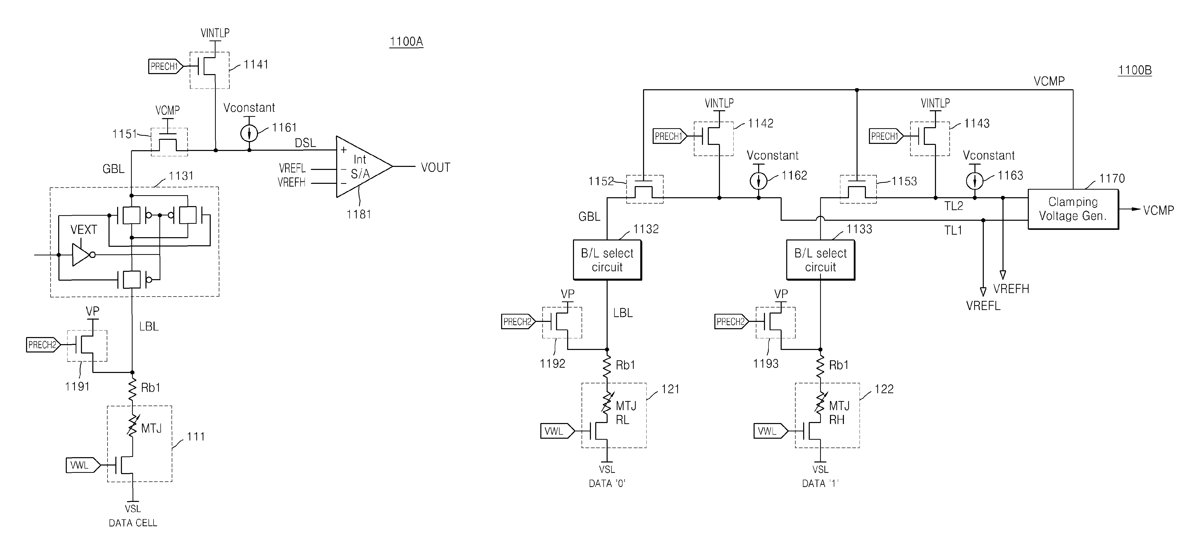
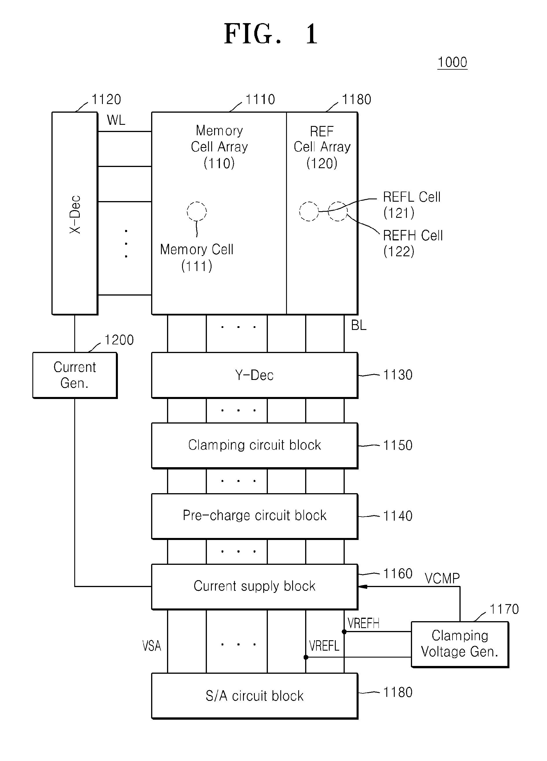
[0030]The described embodiments relate generally to nonvolatile memory devices and ways of improving their performance and / or reliability. For example, one way to improve the reliability of a nonvolatile memory device is by reducing variations in the operation of its memory cells. These variations can be produced by various factors, such as differences in cell resistance values (e.g., in an RRAM), or fluctuations of a bias current, a current source, or a bit line resistance. These variations may also occur due to changes to an external reference voltage applied globally to a memory region.

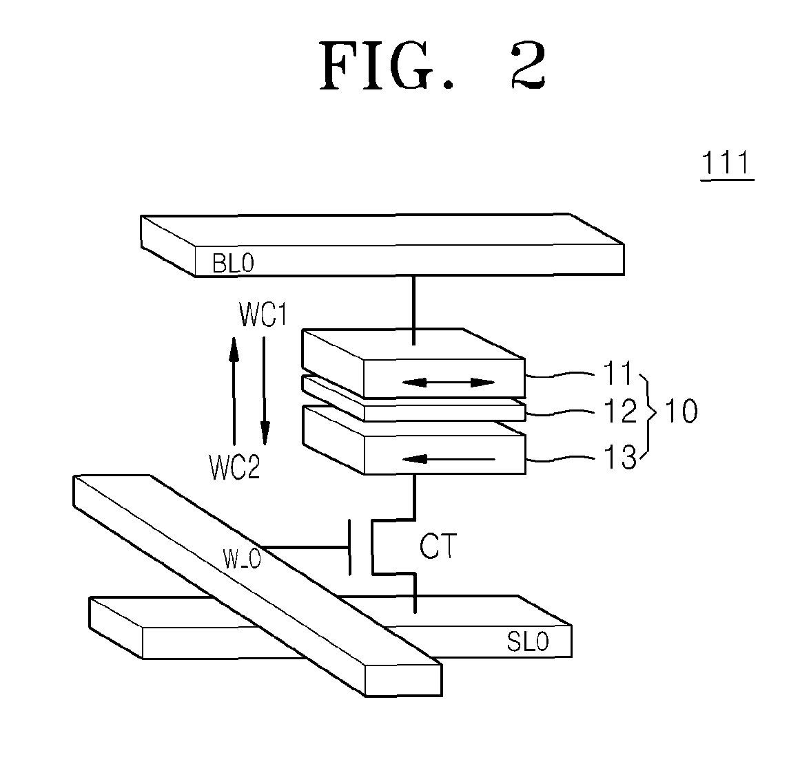
[0031]Certain embodiments are described with reference to an MRAM that stores data using a change in a resistance value of a magnetic tunneling junction (MTJ) ...


PUM


Abstract

A nonvolatile memory device comprises a nonvolatile cell array comprising a memory cell and a reference cell, a clamping circuit electrically connected to the memory cell and configured to clamp a voltage applied to a data sensing line during a read operation, and a clamping voltage generation unit configured to generate a clamping voltage responsive to a first voltage having a level based on the reference cell, and to feed back the clamping voltage to the clamping circuit.

Description

CROSS-REFERENCE TO RELATED APPLICATIONS[0001]This application claims priority under 35 U.S.C. §119 to Korean Patent Application No. 10-2011-0091317 filed on Sep. 8, 2011, the disclosure of which is hereby incorporated by reference in its entirety.BACKGROUND OF THE INVENTION[0002]The inventive concept relates generally to electronic memory technologies. More particularly, the inventive concept relates to a data read circuit, a nonvolatile memory device comprising the data read circuit, and a method of reading data from the nonvolatile memory device.[0003]Semiconductor memory devices can be roughly divided into two categories according to whether they retain stored data when disconnected from power. These categories include volatile memory devices, which lose stored data when disconnected from power, and nonvolatile memory devices, which retain stored data when disconnected from power. Examples of volatile memory devices include static random access memory (SRAM) and dynamic random ac...

Claims


Application Information

Patent Timeline
Patent Type & Authority Patents(United States)
IPC IPC(8): G11C7/02
CPCG11C5/145G11C11/16G11C7/12G11C11/1673G11C16/26G11C16/30G11C7/10G11C7/06
Inventor KIM, CHAN-KYUNGHWANG, HONG-SUNPARK, CHUL-WOOKANG, SANG-BEOMOH, HYUNG-ROK
Owner SAMSUNG ELECTRONICS CO LTD
Why Eureka
Try Eureka